SBOS385B August 2019 – April 2021 INA597
PRODUCTION DATA
- 1 Features
- 2 Applications
- 3 Description
- 4 Revision History
- 5 Device Comparison Table
- 6 Pin Configuration and Functions
- 7 Specifications
- 8 Detailed Description
-
9 Application and Implementation
- 9.1 Application Information
- 9.2
Typical Applications
- 9.2.1 Basic Power-Supply and Signal Connections
- 9.2.2 Precision Instrumentation Amplifier
- 9.2.3 Low Power, High-Output Current, Precision, Difference Amplifier
- 9.2.4 Pseudoground Generator
- 9.2.5 Differential Input Data Acquisition
- 9.2.6 Precision Voltage-to-Current Conversion
- 9.2.7 Additional Applications
- 10Power Supply Recommendations
- 11Layout
- 12Device and Documentation Support
- 13Mechanical, Packaging, and Orderable Information
Package Options
Mechanical Data (Package|Pins)
Thermal pad, mechanical data (Package|Pins)
Orderable Information
6 Pin Configuration and Functions
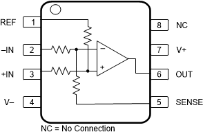
 Figure 6-1 D (8-Pin SOIC) and DGK
(8-Pin VSSOP) Packages, Top View
 Figure 6-2 DRC (10-Pin VSON With
Thermal Pad) Package, Top View
 Table 6-1 Pin Functions
| PIN | I/O | DESCRIPTION | ||
|---|---|---|---|---|
| NAME | D (SOIC), DGK (VSSOP) |
DRC (VSON) | ||
| +IN | 3 | 4 | I | 12-kΩ resistor to noninverting terminal of op amp. Used as positive input in G = ½ configuration. Used as reference pin in G = 2 configuration. |
| –IN | 2 | 3 | I | 12-kΩ resistor to inverting terminal of op amp. Used as negative input in G = ½ configuration. Connect to output in G = 2 configuration. |
| +INOP | — | 10 | I | Direct connection to noninverting terminal of op amp |
| –INOP | — | 1 | I | Direct connection to inverting terminal of op amp |
| NC | 8 | 9 | — | No internal connection (can be left floating) |
| OUT | 6 | 7 | O | Output |
| REF | 1 | 2 | I | 6-kΩ resistor to noninverting terminal of op amp. Used as reference pin in G = ½ configuration. Used as positive input in G = 2 configuration. |
| SENSE | 5 | 6 | I | 6-kΩ resistor to inverting terminal of op amp. Connect to output in G = ½ configuration. Used as negative input in G = 2 configuration. |
| V+ | 7 | 8 | — | Positive (highest) power supply |
| V– | 4 | 5 | — | Negative (lowest) power supply |