SBOS385B August 2019 – April 2021 INA597
PRODUCTION DATA
- 1 Features
- 2 Applications
- 3 Description
- 4 Revision History
- 5 Device Comparison Table
- 6 Pin Configuration and Functions
- 7 Specifications
- 8 Detailed Description
-
9 Application and Implementation
- 9.1 Application Information
- 9.2
Typical Applications
- 9.2.1 Basic Power-Supply and Signal Connections
- 9.2.2 Precision Instrumentation Amplifier
- 9.2.3 Low Power, High-Output Current, Precision, Difference Amplifier
- 9.2.4 Pseudoground Generator
- 9.2.5 Differential Input Data Acquisition
- 9.2.6 Precision Voltage-to-Current Conversion
- 9.2.7 Additional Applications
- 10Power Supply Recommendations
- 11Layout
- 12Device and Documentation Support
- 13Mechanical, Packaging, and Orderable Information
Package Options
Mechanical Data (Package|Pins)
Thermal pad, mechanical data (Package|Pins)
Orderable Information
9.2.1.3 Application Curve
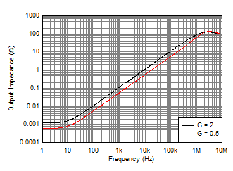
The interaction between the output stage of an operational amplifier (op amp) and capacitive loads can impact the stability of the circuit. Throughout the industry, op-amp output-stage requirements have changed greatly since their original creation. Classic output stages with the class-AB common-emitter bipolar junction transistor (BJT) have now been replaced with common-collector BJT and common-drain complementary metal-oxide semiconductor (CMOS) devices. Both of these technologies enable rail-to-rail output voltages for single-supply and battery-powered applications. A result of changing these output-stage structures is that the op-amp open-loop output impedance (Zo) changed from the largely resistive behavior of early BJT op amps to a frequency-dependent ZO that features capacitive, resistive, and inductive portions. Proper understanding of ZO over frequency—and also the resulting closed-loop output impedance over frequency—is crucial for the understanding of loop gain, bandwidth, and stability analysis. Figure 9-4 shows how the INA597 closed-loop output impedance varies over frequency.

| VS = ±18 V |