SBOS160A November 1993 – January 2015 ISO122
PRODUCTION DATA.
- 1 Features
- 2 Applications
- 3 Description
- 4 Simplified Schematic
- 5 Revision History
- 6 Pin Configuration and Functions
- 7 Specifications
- 8 Detailed Description
-
9 Application and Implementation
- 9.1 Application Information
- 9.2 Typical Application
- 10Power Supply Recommendations
- 11Layout
- 12Device and Documentation Support
- 13Mechanical, Packaging, and Orderable Information
Package Options
Mechanical Data (Package|Pins)
Thermal pad, mechanical data (Package|Pins)
Orderable Information
9 Application and Implementation
NOTE
Information in the following applications sections is not part of the TI component specification, and TI does not warrant its accuracy or completeness. TI’s customers are responsible for determining suitability of components for their purposes. Customers should validate and test their design implementation to confirm system functionality.
9.1 Application Information
9.1.1 Carrier Frequency Considerations
The ISO122 amplifier transmits the signal across the isolation barrier by a 500kHz duty cycle modulation technique. For input signals having frequencies below 250 kHz, this system works like any linear amplifier. But for frequencies above 250 kHz, the behavior is similar to that of a sampling amplifier. The signal response to inputs greater than 250 kHz performance curve shows this behavior graphically; at input frequencies above
250 kHz the device generates an output signal component of reduced magnitude at a frequency below 250 kHz. This is the aliasing effect of sampling at frequencies less than two times the signal frequency (the Nyquist frequency). At the carrier frequency and its harmonics, both the frequency and amplitude of the aliasing go to zero.
9.1.2 Isolation Mode Voltage Induced Errors
IMV can induce errors at the output as indicated by the plots of IMV vs Frequency. It should be noted that if the IMV frequency exceeds 250 kHz, the output also will display spurious outputs (aliasing), in a manner similar to that for VIN > 250 kHz and the amplifier response will be identical to that shown in the Signal Response to Inputs Greater Than 250-kHz performance curve. This occurs because IMV-induced errors behave like input-referred error signals. To predict the total error, divide the isolation voltage by the IMR shown in the IMR vs Frequency curve and compute the amplifier response to this input-referred error signal from the data given in the Signal Response to Inputs Greater than 250-kHz performance curve. For example, if a 800-kHz 1000-Vrms IMR is present, then a total of [(–60 dB) + (–30 dB)] x (1000 V) = 32-mV error signal at 200 kHz plus a 1 V, 800-kHz error signal will be present at the output.
9.1.3 High IMV dV/dt Errors
As the IMV frequency increases and the dV/dt exceeds 1000 Vµs, the sense amp may start to false trigger, and the output will display spurious errors. The common-mode current being sent across the barrier by the high slew rate is the cause of the false triggering of the sense amplifier. Lowering the power-supply voltages below ±15 V may decrease the dV/dt to 500 V/µs for typical performance.
9.1.4 High Voltage Testing
Texas Instruments has adopted a partial discharge test criterion that conforms to the German VDE0884 Optocoupler Standards. This method requires the measurement of minute current pulses (< 5 pC) while applying 2400-Vrms, 60-Hz high-voltage stress across every ISO122 isolation barrier. No partial discharge may be initiated to pass this test. This criterion confirms transient overvoltage (1.6 × 1500 Vrms) protection without damage to the ISO122. Lifetest results verify the absence of failure under continuous rated voltage and maximum temperature.
This new test method represents the “state of the art” for nondestructive high–voltage reliability testing. It is based on the effects of nonuniform fields that exist in heterogeneous dielectric material during barrier degradation. In the case of void nonuniformities, electric field stress begins to ionize the void region before bridging the entire high-voltage barrier. The transient conduction of charge during and after the ionization can be detected externally as a burst of 0.01–0.1 ms current pulses that repeat on each AC voltage cycle. The minimum AC barrier voltage that initiates partial discharge is defined as the “inception voltage.” Decreasing the barrier voltage to a lower level is required before partial discharge ceases and is defined as the “extinction voltage.” The package insulation processes have been characterized and developed to yield an inception voltage in excess of 2400 Vrms so that transient overvoltages below this level will not damage the ISO122. The extinction voltage is above 1500 Vrms so that even overvoltage induced partial discharge will cease once the barrier voltage is reduced to the 1500 Vrms (rated) level. Older high-voltage test methods relied on applying a large enough overvoltage (above rating) to break down marginal parts, but not so high as to damage good ones. Our new partial discharge testing gives us more confidence in barrier reliability than breakdown/no breakdown criteria.
9.2 Typical Application
9.2.1 Output Filter
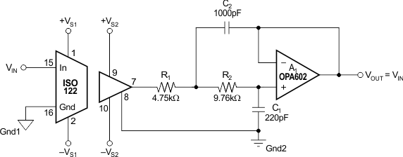 Figure 10. ISO122 With Output Filter for Improved Ripple
9.2.1.1 Design Requirements
The ISO122 isolation amplifiers (ISO amps) have a small (10 to 20 mVp-p typical) residual demodulator ripple at the output. A simple filter can be added to eliminate the output ripple without decreasing the 50-kHz signal bandwidth of the ISO amp.
9.2.1.2 Detailed Design Procedure
The ISO122 is designed to have a 50-kHz single-pole (Butterworth) signal response. By cascading the ISO amp with a simple 50-kHz, Q = 1, two-pole, low-pass filter, the overall signal response becomes three-pole Butterworth. The result is a maximally flat 50-kHz magnitude response and the output ripple reduced below the noise level. Figure 10 shows the complete circuit. The two-pole filter is a unity-gain Sallen-Key type consisting of A1, R1, R2, C1, and C2. The values shown give Q = 1 and f–3-dB bandwidth = 50 kHz. Because the op amp is connected as a unity-gain follower, gain and gain accuracy of the ISO amp are unaffected. Using a precision op amp such as the OPA602 also preserves the DC accuracy of the ISO amp.
9.2.1.3 Application Curves
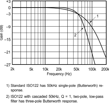 Figure 11. Gain vs. Frequency
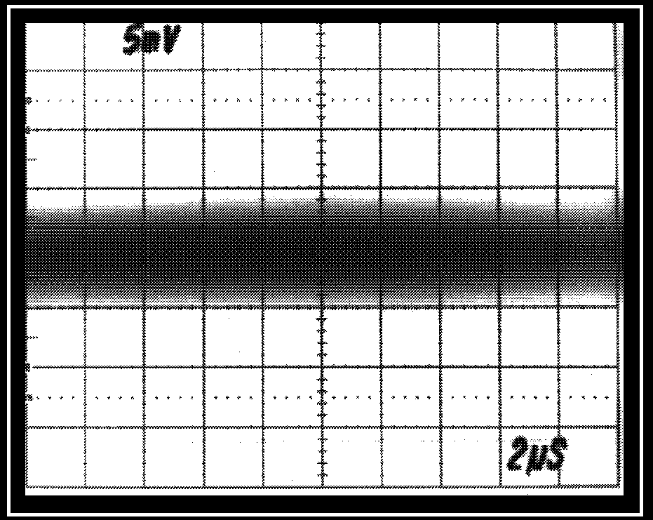 Figure 13. Filtered ISO122 (No Visible Output Ripple)
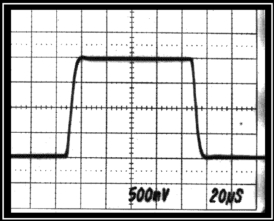 Figure 15. Step Response of ISO122 With Added Twopole Output Filter
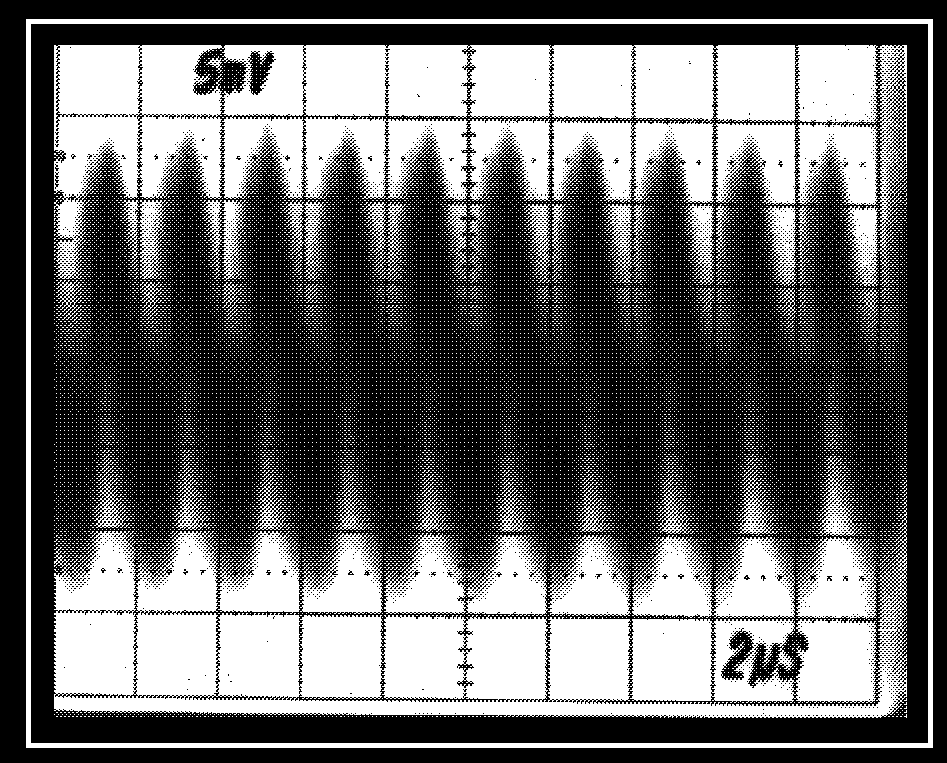
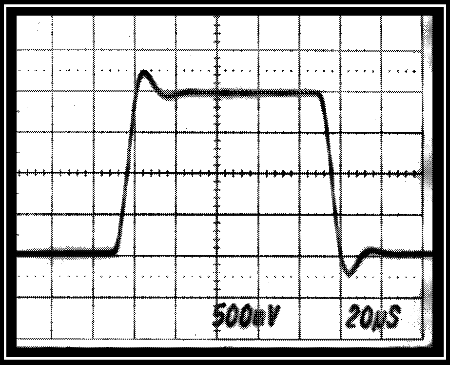 Figure 14. Step Response of Standard ISO122
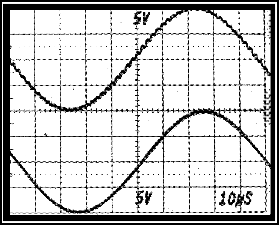 Figure 16. Large-signal, 10 kHz Sine-wave Response of ISO122 With and Without Output Filter
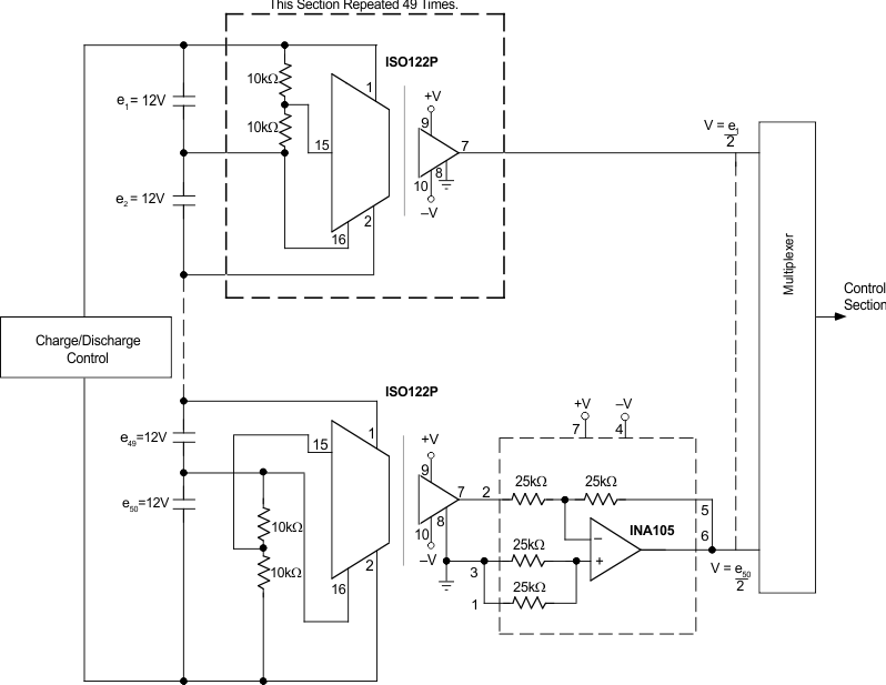
9.2.2 Battery Monitor
Figure 17 provides a means to monitor the cell voltage on a 600-V battery stack by using the battery as a power source for the isolated voltage.
9.2.3 Programmable Gain Amplifier
In applications where variable gain configurations are required, a programmable gain amplifier like the PGA102 can be used with the ISO122. Figure 18 uses an ISO150 to provide gain pin selection options to the PGA102.
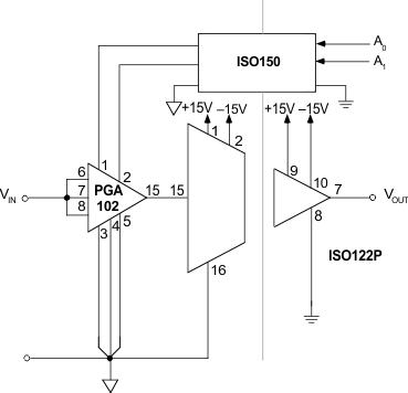 Figure 18. Programmable-Gain Isolation Channel With Gains of 1, 10, and 100
9.2.4 Thermocouple Amplifier
For isolated temperature measurements, Figure 19 provides an application solution using the INA101 feeding the input stage of the ISO122. The table provides suggested resistor values based on the type of thermistor used in the application.
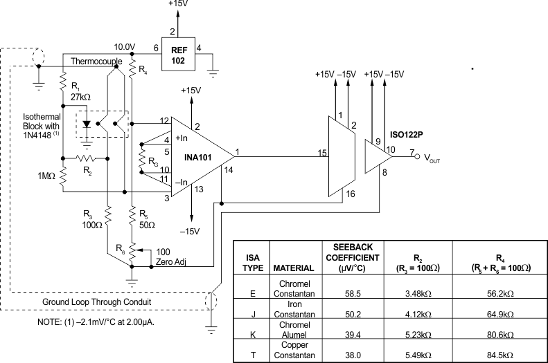 Figure 19. Thermocouple Amplifier With Ground Loop Elimination,
 Cold Junction Compensation, and Up-scale Burn-out.
9.2.5 Isolated 4- to 20-mA Instrument Loop
For isolated temperature measurements in a 4- to 20-mA loop, Figure 20 provides a solution using the XTR101 and RCV420. A high-performance PT100 resistance temperature detector (RTD) provides the user with an isolated 0- to 5-V representation of the isolated temperature measurement.
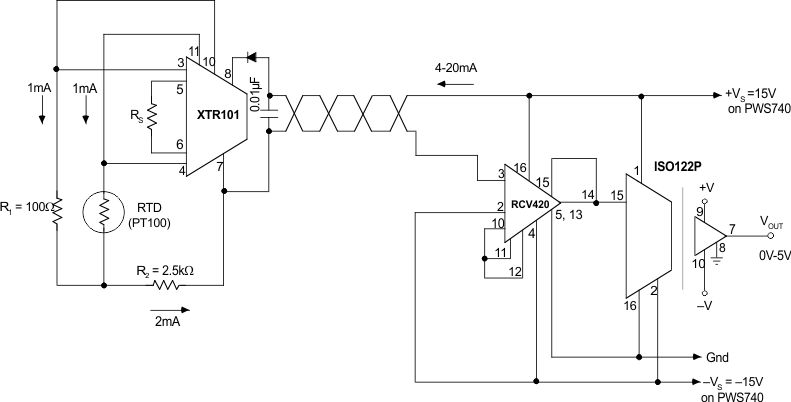 Figure 20. Isolated 4- to 200-mA Instrument Loop. (RTD shown.)
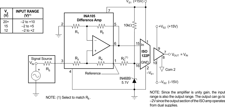
9.2.6 Single-Supply Operation of the ISO122P Isolation Amplifier
The circuit shown in Figure 21 uses a 5.1-V Zener diode to generate the negative supply for an ISO122 from a single supply on the high-voltage side of the isolation amplifier. The input measuring range will be dependent on the applied voltage as noted in the accompanying table.
9.2.7 Input-Side Powered ISO Amp
The user side of the ISO122 can be powered from the high-voltage side using an isolated DC-DC converter as shown in Figure 22.
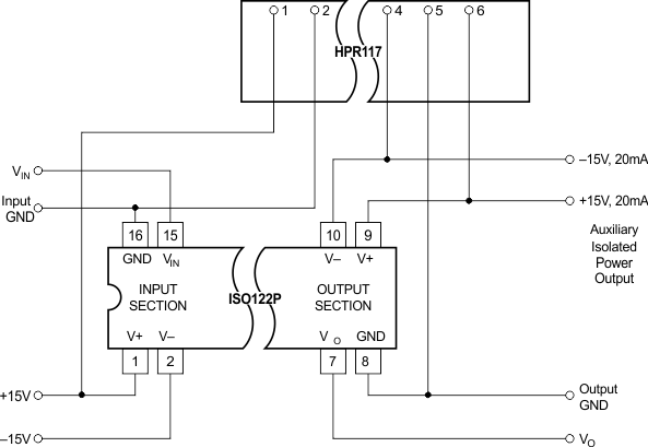 Figure 22. Input-Side Powered ISO Amp
9.2.8 Powered ISO Amp With Three-Port Isolation
Figure 23 shows an application solution that provides isolated power to both the user and high-voltage sides of the ISO122 amplifier.
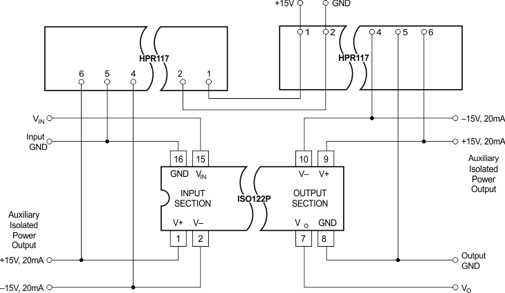 Figure 23. Powered ISO Amp With Three-Port Isolation