SBOS160A November   1993  – January 2015 ISO122

PRODUCTION DATA.  

  1. Features
  2. Applications
  3. Description
  4. Simplified Schematic
  5. Revision History
  6. Pin Configuration and Functions
  7. Specifications
    1. 7.1 Absolute Maximum Ratings
    2. 7.2 ESD Ratings
    3. 7.3 Recommended Operating Conditions
    4. 7.4 Thermal Information
    5. 7.5 Electrical Characteristics
    6. 7.6 Typical Characteristics
  8. Detailed Description
    1. 8.1 Overview
      1. 8.1.1 Modulator
      2. 8.1.2 Demodulator
    2. 8.2 Functional Block Diagram
    3. 8.3 Feature Description
      1. 8.3.1 Isolation Amplifier
    4. 8.4 Device Functional Modes
  9. Application and Implementation
    1. 9.1 Application Information
      1. 9.1.1 Carrier Frequency Considerations
      2. 9.1.2 Isolation Mode Voltage Induced Errors
      3. 9.1.3 High IMV dV/dt Errors
      4. 9.1.4 High Voltage Testing
    2. 9.2 Typical Application
      1. 9.2.1 Output Filter
        1. 9.2.1.1 Design Requirements
        2. 9.2.1.2 Detailed Design Procedure
        3. 9.2.1.3 Application Curves
      2. 9.2.2 Battery Monitor
      3. 9.2.3 Programmable Gain Amplifier
      4. 9.2.4 Thermocouple Amplifier
      5. 9.2.5 Isolated 4- to 20-mA Instrument Loop
      6. 9.2.6 Single-Supply Operation of the ISO122P Isolation Amplifier
      7. 9.2.7 Input-Side Powered ISO Amp
      8. 9.2.8 Powered ISO Amp With Three-Port Isolation
  10. 10Power Supply Recommendations
    1. 10.1 Signal and Supply Connections
  11. 11Layout
    1. 11.1 Layout Guidelines
    2. 11.2 Layout Example
  12. 12Device and Documentation Support
    1. 12.1 Trademarks
    2. 12.2 Electrostatic Discharge Caution
    3. 12.3 Glossary
  13. 13Mechanical, Packaging, and Orderable Information

Package Options

Mechanical Data (Package|Pins)
Thermal pad, mechanical data (Package|Pins)
Orderable Information

11 Layout

11.1 Layout Guidelines

To maintain the isolation barrier of the device, the distance between the high-side ground (pin 16 or 28) and the low-side ground (pin 8 or 14) should be kept at maximum; that is, the entire area underneath the device should be kept free of any conducting materials.

11.2 Layout Example

ISO12xU_layout.gif
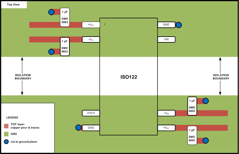
Figure 25. Typical Layout