SLLSF40B November 2017 – September 2019 ISOW7821
PRODUCTION DATA.
- 1 Features
- 2 Applications
- 3 Description
- 4 Revision History
- 5 Description (continued)
- 6 Pin Configuration and Functions
-
7 Specifications
- 7.1 Absolute Maximum Ratings
- 7.2 ESD Ratings
- 7.3 Recommended Operating Conditions
- 7.4 Thermal Information
- 7.5 Power Ratings
- 7.6 Insulation Specifications
- 7.7 Safety-Related Certifications
- 7.8 Safety Limiting Values
- 7.9 Electrical Characteristics—5-V Input, 5-V Output
- 7.10 Supply Current Characteristics—5-V Input, 5-V Output
- 7.11 Electrical Characteristics—5-V Input, 3.3-V Output
- 7.12 Supply Current Characteristics—5-V Input, 3.3-V Output
- 7.13 Electrical Characteristics—3.3-V Input, 3.3-V Output
- 7.14 Supply Current Characteristics—3.3-V Input, 3.3-V Output
- 7.15 Switching Characteristics—5-V Input, 5-V Output
- 7.16 Switching Characteristics—5-V Input, 3.3-V Output
- 7.17 Switching Characteristics—3.3-V Input, 3.3-V Output
- 7.18 Insulation Characteristics Curves
- 7.19 Typical Characteristics
- 8 Parameter Measurement Information
- 9 Detailed Description
- 10Application and Implementation
- 11Power Supply Recommendations
- 12Layout
- 13Device and Documentation Support
- 14Mechanical, Packaging, and Orderable Information
Package Options
Mechanical Data (Package|Pins)
- DWE|16
Thermal pad, mechanical data (Package|Pins)
Orderable Information
10.2.2 Detailed Design Procedure
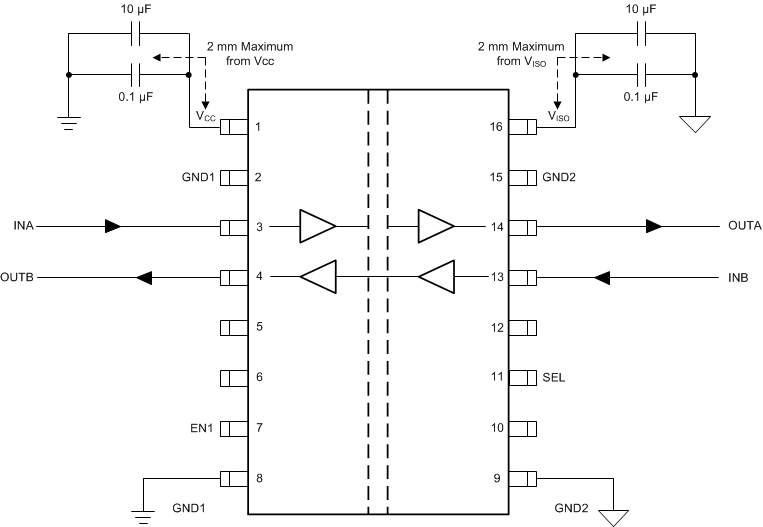
The ISOW7821 device only requires external bypass capacitors to operate. These low-ESR ceramic bypass capacitors must be placed as close to the chip pads as possible.

Optional 100 µF capacitor can be added between VCC and GND1; refer to Power Supply Recommendations.
Figure 31. Typical Circuit Hook-Up The VCC power-supply input provides power to isolated data channels and to the isolated DC-DC converter. Use Equation 1 to calculate the total power budget on the primary side.
Equation 1. ICC = (VISO × IISO) / (η × VCC) + Iinpx
where
- ICC is the total current required by the primary supply.
- VISO is the isolated supply voltage.
- IISO is the external load on the isolated supply voltage.
- η is the efficiency.
- VCC is the supply voltage.
- Iinpx is the total current drawn for the isolated data channels and power converter when data channels are toggling at a specific data rate. This data is shown in the Electrical Characteristics—5-V Input, 5-V Output table.