SNOSBI3C July 2000 – October 2018 LF198-N , LF298 , LF398-N
PRODUCTION DATA.
- 1 Features
- 2 Applications
- 3 Description
- 4 Revision History
- 5 Pin Configuration and Functions
-
6 Specifications
- 6.1 Absolute Maximum Ratings
- 6.2 Recommended Operating Conditions
- 6.3 Thermal Information
- 6.4 Electrical Characteristics, LF198-N and LF298
- 6.5 Electrical Characteristics, LF198A-N
- 6.6 Electrical Characteristics, LF398-N
- 6.7 Electrical Characteristics, LF398A-N (OBSOLETE)
- 6.8 Typical Characteristics
- 7 Parameter Measurement Information
- 8 Detailed Description
-
9 Application and Implementation
- 9.1 Application Information
- 9.2
Typical Applications
- 9.2.1 X1000 Sample and Hold
- 9.2.2 Sample and Difference Circuit
- 9.2.3 Ramp Generator With Variable Reset Level
- 9.2.4 Integrator With Programmable Reset Level
- 9.2.5 Output Holds at Average of Sampled Input
- 9.2.6 Increased Slew Current
- 9.2.7 Reset Stabilized Amplifier
- 9.2.8 Fast Acquisition, Low Droop Sample and Hold
- 9.2.9 Synchronous Correlator for Recovering Signals Below Noise Level
- 9.2.10 2-Channel Switch
- 9.2.11 DC and AC Zeroing
- 9.2.12 Staircase Generator
- 9.2.13 Differential Hold
- 9.2.14 Capacitor Hysteresis Compensation
- 10Power Supply Recommendations
- 11Layout
- 12Device and Documentation Support
- 13Mechanical, Packaging, and Orderable Information
Package Options
Mechanical Data (Package|Pins)
- LMC|8
Thermal pad, mechanical data (Package|Pins)
Orderable Information
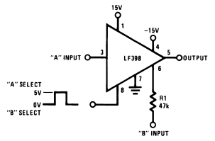
9.2.10 2-Channel Switch
The HOLD CAPACITOR pin could be alternatively used as a second input to create a 2-channel switch shown Figure 36
 Figure 36. 2-Channel Switch
 In the configuration of Figure 36, input signal A and input signal B have the characteristics listed in Table 1.
Table 1. 2-Channel Switch Characteristics
| A | B | |
|---|---|---|
| Gain | 1 ± 0.02% | 1 ± 0.2% |
| ZIN | 1010 Ω | 47 kΩ |
| BW | ≈1 MHz | ≈400 kHz |
| Crosstalk @ 1 kHz | –90 dB | –90 dB |
| Offset | ≤ 6 mV | ≤ 75 mV |