SNVS625G February   2011  – March 2022 LM21215

PRODUCTION DATA  

  1. Features
  2. Applications
  3. Description
  4. Revision History
  5. Pin Configuration and Functions
  6. Specifications
    1. 6.1 Absolute Maximum Ratings
    2. 6.2 ESD Ratings
    3. 6.3 Recommended Operating Ratings
    4. 6.4 Electrical Characteristics
    5. 6.5 Typical Characteristics
  7. Detailed Description
    1. 7.1 Overview
    2. 7.2 Functional Block Diagram
    3. 7.3 Feature Description
      1. 7.3.1 Precision Enable
      2. 7.3.2 UVLO
      3. 7.3.3 Current Limit
      4. 7.3.4 Short-Circuit Protection
      5. 7.3.5 Thermal Protection
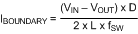
      6. 7.3.6 Light Load Operation
      7. 7.3.7 Power Good Flag
    4. 7.4 Device Functional Modes
  8. Application and Implementation
    1. 8.1 Application Information
    2. 8.2 Typical Application
      1. 8.2.1 Typical Application 1
        1. 8.2.1.1 Design Requirements
        2. 8.2.1.2 Detailed Design Procedure
          1. 8.2.1.2.1 Custom Design With WEBENCH® Tools
          2. 8.2.1.2.2 Output Voltage
          3. 8.2.1.2.3 Precision Enable
          4. 8.2.1.2.4 Soft Start
          5. 8.2.1.2.5 Inductor Selection
          6. 8.2.1.2.6 Output Capacitor Selection
          7. 8.2.1.2.7 Input Capacitor Selection
          8. 8.2.1.2.8 Programmable Current Limit
          9. 8.2.1.2.9 Control Loop Compensation
        3. 8.2.1.3 Application Curves
      2. 8.2.2 Typical Application Schematic 2
        1. 8.2.2.1 Design Requirements
        2. 8.2.2.2 Detailed Design Procedure
  9. Layout
    1. 9.1 Layout Considerations
    2. 9.2 Layout Example
      1. 9.2.1 Thermal Considerations
  10. 10Device and Documentation Support
    1. 10.1 Device Support
      1. 10.1.1 Third-Party Products Disclaimer
      2. 10.1.2 Development Support
        1. 10.1.2.1 Custom Design With WEBENCH® Tools
    2. 10.2 Receiving Notification of Documentation Updates
    3. 10.3 Support Resources
    4. 10.4 Trademarks
    5. 10.5 Electrostatic Discharge Caution
    6. 10.6 Glossary
  11. 11Mechanical, Packaging, and Orderable Information

Package Options

Mechanical Data (Package|Pins)
Thermal pad, mechanical data (Package|Pins)
Orderable Information

Light Load Operation

The LM21215 offers increased efficiency when operating at light loads. Whenever the load current is reduced to a point where the peak to peak inductor ripple current is greater than two times the load current, the device will enter the diode emulation mode, preventing significant negative inductor current. The point at which this occurs is the critical conduction boundary and can be calculated with Equation 1:

Equation 1. GUID-11EE8562-BCFA-41D5-9692-CC782B275EF1-low.gif

It can be seen that in diode emulation mode, whenever the inductor current reaches zero, the SW node becomes high impedance. Ringing will occur on this pin as a result of the LC tank circuit formed by the inductor and the parasitic capacitance at the node. If this ringing is of concern, an additional RC snubber circuit can be added from the switch node to ground.

At very light loads, usually below 100 mA, several pulses can be skipped in between switching cycles, effectively reducing the switching frequency and further improving light-load efficiency.