SNVS625G February 2011 – March 2022 LM21215
PRODUCTION DATA
- 1 Features
- 2 Applications
- 3 Description
- 4 Revision History
- 5 Pin Configuration and Functions
- 6 Specifications
- 7 Detailed Description
- 8 Application and Implementation
- 9 Layout
- 10Device and Documentation Support
- 11Mechanical, Packaging, and Orderable Information
Package Options
Mechanical Data (Package|Pins)
- PWP|20
Thermal pad, mechanical data (Package|Pins)
- PWP|20
Orderable Information
8.2.1.2.9 Control Loop Compensation
The LM21215 incorporates a high bandwidth amplifier between the FB and COMP pins to allow the user to design a compensation network that matches the application. This section will walk through the various steps in obtaining the open loop transfer function.
There are three main blocks of a voltage mode buck switcher that the power supply designer must consider when designing the control system: the power train, modulator, and the compensated error amplifier. A closed loop diagram is shown in Figure 8-6.
 Figure 8-6 Loop Diagram
The power train consists of the output inductor (L) with DCR (DC resistance RDCR), output capacitor (C0) with ESR (effective series resistance RESR), and load resistance (Ro). The error amplifier (EA) constantly forces FB to 0.6 V. The passive compensation components around the error amplifier help maintain system stability. The modulator creates the duty cycle by comparing the error amplifier signal with an internally generated ramp set at the switching frequency.
There are three transfer functions that must be taken into consideration when obtaining the total open loop transfer function: COMP to SW (modulator), SW to VOUT (power train), and VOUT to COMP (error amplifier). The COMP to SW transfer function is simply the gain of the PWM modulator.

where
- ΔVRAMP is the oscillator peak-to-peak ramp voltage (nominally 0.8 V).
The SW to COMP transfer function includes the output inductor, output capacitor, and output load resistance. The inductor and capacitor create two complex poles at a frequency described by:
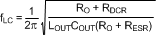
In addition to two complex poles, a left half plane zero is created by the output capacitor ESR located at a frequency described by:

A Bode plot showing the power train response can be seen in Figure 8-7.
 Figure 8-7 Power Train Bode Plot
The complex poles created by the output inductor and capacitor cause a 180° phase shift at the resonant frequency as seen in Figure 8-7. The phase is boosted back up to –90° due to the output capacitor ESR zero. The 180° phase shift must be compensated out and phase boosted through the error amplifier to stabilize the closed loop response. The compensation network shown around the error amplifier in Figure 8-6 creates two poles, two zeros, and a pole at the origin. Placing these poles and zeros at the correct frequencies stabilizes the closed loop response. The Compensated Error Amplifier transfer function is:
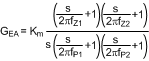
The pole located at the origin gives high open loop gain at DC, translating into improved load regulation accuracy. This pole occurs at a very low frequency due to the limited gain of the error amplifier, however, it can be approximated at DC for the purposes of compensation. The other two poles and two zeros can be located accordingly to stabilize the voltage mode loop depending on the power stage complex poles and Q. Figure 8-8 is an illustration of what the Error Amplifier Compensation transfer function will look like.
 Figure 8-8 Type 3 Compensation Network Bode Plot
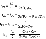
As seen in Figure 8-8, the two zeros (fLC/2, fLC) in the compensation network give a phase boost. This will cancel out the effects of the phase loss from the output filter. The compensation network also adds two poles to the system. One pole should be located at the zero caused by the output capacitor ESR (fESR), and the other pole must be at half the switching frequency (fSW/2) to roll off the high frequency response. The dependency of the pole and zero locations on the compensation components is described in Equation 16.
An example of the step-by-step procedure to generate compensation component values using the typical application setup, is given. The parameters needed for the compensation values are given in Table 8-2.
| PARAMETER | VALUE |
|---|---|
| VIN | 5 V |
| VOUT | 1.2 V |
| IOUT | 15 A |
| fCROSSOVER | 100 kHz |
| L | 0.56 µH |
| RDCR | 1.8 mΩ |
| CO | 150 µF |
| RESR | 1.0 mΩ |
| ΔVRAMP | 0.8 V |
| fSW | 500 kHz |
where ΔVRAMP is the oscillator peak-to-peak ramp voltage (nominally 0.8 V), and fCROSSOVER is the frequency at which the open-loop gain is a magnitude of 1. It is recommended that the fCROSSOVER not exceed one-fifth of the switching frequency. The output capacitance, CO, depends on capacitor chemistry and bias voltage. For multi-layer ceramic capacitors (MLCC), the total capacitance will degrade as the DC bias voltage is increased. Measuring the actual capacitance value for the output capacitors at the output voltage is recommended to accurately calculate the compensation network. The example given here is the total output capacitance using the three MLCC output capacitors biased at 1.2 V, as seen in Figure 8-1. Note that it is more conservative, from a stability standpoint, to err on the side of a smaller output capacitance value in the compensation calculations rather than a larger, as this will result in a lower bandwidth but increased phase margin.
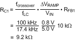
First, the value of RFB1 should be chosen. A typical value is 10 kΩ. From this, the value of RC1 can be calculated to set the mid-band gain so that the desired crossover frequency is achieved:
Next, the value of CC1 can be calculated by placing a zero at half of the LC double pole frequency (fLC):

Now the value of CC2 can be calculated to place a pole at half of the switching frequency (fSW):
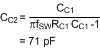
RC2 can then be calculated to set the second zero at the LC double pole frequency:

Last, CC3 can be calculated to place a pole at the same frequency as the zero created by the output capacitor ESR:

An illustration of the total loop response can be seen in Figure 8-9.
 Figure 8-9 Loop Response
It is important to verify the stability by either observing the load transient response or by using a network analyzer. A phase margin between 45° and 70° is usually desired for voltage mode systems. Excessive phase margin can cause slow system response to load transients and low phase margin can cause an oscillatory load transient response. If the load step response peak deviation is larger than desired, increasing fCROSSOVER and recalculating the compensation components can help, but usually at the expense of phase margin.