SNVS581M February 2013 – October 2020 LM22679 , LM22679-Q1
PRODUCTION DATA
- 1 Features
- 2 Applications
- 3 Description
- 4 Revision History
- 5 Pin Configuration and Functions
- 6 Specifications
- 7 Detailed Description
- 8 Application and Implementation
- 9 Power Supply Recommendations
- 10Layout
- 11Device and Documentation Support
Package Options
Mechanical Data (Package|Pins)
- NDR|7
Thermal pad, mechanical data (Package|Pins)
Orderable Information
7.4.6 Duty-Cycle Limits
Ideally the regulator would control the duty cycle over the full range of zero to one. However due to inherent delays in the circuitry, there are limits on both the maximum and minimum duty cycles that can be reliably controlled. This in turn places limits on the maximum and minimum input and output voltages that can be converted by the LM22679. A minimum on-time is imposed by the regulator in order to correctly measure the switch current during a current limit event. A minimum off-time is imposed in order the re-charge the bootstrap capacitor. Equation 7 can be used to determine the approximate maximum input voltage for a given output voltage.
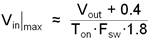
where
- Fsw is the switching frequency
- TON is the minimum on-time
Both parameters are found in Section 6.6.
Nominal values should be used. The worst case is lowest output voltage. If this input voltage is exceeded, the regulator will skip cycles, effectively lowering the switching frequency. The consequences of this are higher output voltage ripple and a degradation of the output voltage accuracy.
The second limitation is the maximum duty cycle before the output voltage will "dropout" of regulation. Equation 8 can be used to approximate the minimum input voltage before dropout occurs:
where

- The values of TOFF and RDS(ON) are found in Section 6.6.
The worst case here is largest load. In this equation, RL is the dc inductor resistance. Of course, the lowest input voltage to the regulator must not be less than 4.5 V (typ).