SNVS107G June   1999  – March 2023 LM2576 , LM2576HV

PRODUCTION DATA  

  1. Features
  2. Applications
  3. Description
  4. Revision History
  5. Pin Configuration and Functions
  6. Specifications
    1. 6.1  Absolute Maximum Ratings
    2. 6.2  ESD Ratings
    3. 6.3  Recommended Operating Conditions
    4. 6.4  Thermal Information
    5. 6.5  Electrical Characteristics: 3.3 V
    6. 6.6  Electrical Characteristics: 5 V
    7. 6.7  Electrical Characteristics: 12 V
    8. 6.8  Electrical Characteristics: 15 V
    9. 6.9  Electrical Characteristics: Adjustable Output Voltage
    10. 6.10 Electrical Characteristics: All Output Voltage Versions
    11. 6.11 Typical Characteristics
  7. Detailed Description
    1. 7.1 Overview
    2. 7.2 Functional Block Diagram
    3. 7.3 Feature Description
      1. 7.3.1 Undervoltage Lockout
      2. 7.3.2 Delayed Start-Up
      3. 7.3.3 Adjustable Output, Low-Ripple Power Supply
    4. 7.4 Device Functional Modes
      1. 7.4.1 Shutdown Mode
      2. 7.4.2 Active Mode
      3. 7.4.3 Current Limit
  8. Application and Implementation
    1. 8.1 Application Information
      1. 8.1.1  Input Capacitor (CIN)
      2. 8.1.2  Inductor Selection
      3. 8.1.3  Inductor Ripple Current
      4. 8.1.4  Output Capacitor
      5. 8.1.5  Catch Diode
      6. 8.1.6  Output Voltage Ripple and Transients
      7. 8.1.7  Feedback Connection
      8. 8.1.8  ON /OFF INPUT
      9. 8.1.9  Inverting Regulator
      10. 8.1.10 Negative Boost Regulator
    2. 8.2 Typical Applications
      1. 8.2.1 Fixed Output Voltage Version
        1. 8.2.1.1 Design Requirements
        2. 8.2.1.2 Detailed Design Procedure
          1. 8.2.1.2.1 Custom Design with WEBENCH® Tools
          2. 8.2.1.2.2 Inductor Selection (L1)
          3. 8.2.1.2.3 Output Capacitor Selection (COUT)
          4. 8.2.1.2.4 Catch Diode Selection (D1)
          5. 8.2.1.2.5 Input Capacitor (CIN)
        3. 8.2.1.3 Application Curves
      2. 8.2.2 Adjusted Output Voltage Version
        1. 8.2.2.1 Design Requirements
        2. 8.2.2.2 Detailed Design Procedure
          1. 8.2.2.2.1 Programming Output Voltage
          2. 8.2.2.2.2 Inductor Selection (L1)
          3. 8.2.2.2.3 Output Capacitor Selection (COUT)
          4. 8.2.2.2.4 Catch Diode Selection (D1)
          5. 8.2.2.2.5 Input Capacitor (CIN)
    3. 8.3 Power Supply Recommendations
    4. 8.4 Layout
      1. 8.4.1 Layout Guidelines
      2. 8.4.2 Layout Example
      3. 8.4.3 Grounding
      4. 8.4.4 Heat Sink and Thermal Considerations
  9. Device and Documentation Support
    1. 9.1 Device Support
      1. 9.1.1 Device Nomenclature
        1. 9.1.1.1 Definition of Terms
      2. 9.1.2 Development Support
        1. 9.1.2.1 Custom Design with WEBENCH® Tools
    2. 9.2 Documentation Support
      1. 9.2.1 Related Documentation
    3. 9.3 Support Resources
    4. 9.4 Receiving Notification of Documentation Updates
    5. 9.5 Trademarks
    6. 9.6 Electrostatic Discharge Caution
    7. 9.7 Glossary
  10. 10Mechanical, Packaging, and Orderable Information

Package Options

Refer to the PDF data sheet for device specific package drawings

Mechanical Data (Package|Pins)
  • NDH|5
  • NEB|5
  • KTT|5
  • KC|5
Thermal pad, mechanical data (Package|Pins)
Orderable Information
Inductor Selection (L1)
  1. Calculate the inductor Volt • microsecond constant, E • T (V • μs), from Equation 9:
    Equation 9. GUID-814A9980-8AEA-4289-BDA0-20783F9C8BAA-low.gif

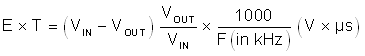
    Calculate E • T (V • μs)

    Equation 10. GUID-4560F2EF-C477-4FEF-9C15-11EC538E3247-low.gif
  2. Use the E • T value from the previous formula and match it with the E • T number on the vertical axis of the Inductor value selection guide shown in Figure 8-8.

    E • T = 115 V • μs

  3. On the horizontal axis, select the maximum load current.

    ILOAD(Max) = 3 A

  4. Identify the inductance region intersected by the E • T value and the maximum load current value, and note the inductor code for that region.

    Inductance Region = H150

  5. Identify the inductor value from the inductor code, and select an appropriate inductor from the table shown in Table 8-4. Part numbers are listed for three inductor manufacturers. The inductor chosen must be rated for operation at the LM2576 switching frequency (52 kHz) and for a current rating of 1.15 × ILOAD. For additional inductor information, see Section 8.1.2.

    Inductor Value = 150 μH

    Choose from AIE part #415-0936, Pulse Engineering part #PE-531115, or Renco part #RL2445.