SNVS107G June   1999  – March 2023 LM2576 , LM2576HV

PRODUCTION DATA  

  1. Features
  2. Applications
  3. Description
  4. Revision History
  5. Pin Configuration and Functions
  6. Specifications
    1. 6.1  Absolute Maximum Ratings
    2. 6.2  ESD Ratings
    3. 6.3  Recommended Operating Conditions
    4. 6.4  Thermal Information
    5. 6.5  Electrical Characteristics: 3.3 V
    6. 6.6  Electrical Characteristics: 5 V
    7. 6.7  Electrical Characteristics: 12 V
    8. 6.8  Electrical Characteristics: 15 V
    9. 6.9  Electrical Characteristics: Adjustable Output Voltage
    10. 6.10 Electrical Characteristics: All Output Voltage Versions
    11. 6.11 Typical Characteristics
  7. Detailed Description
    1. 7.1 Overview
    2. 7.2 Functional Block Diagram
    3. 7.3 Feature Description
      1. 7.3.1 Undervoltage Lockout
      2. 7.3.2 Delayed Start-Up
      3. 7.3.3 Adjustable Output, Low-Ripple Power Supply
    4. 7.4 Device Functional Modes
      1. 7.4.1 Shutdown Mode
      2. 7.4.2 Active Mode
      3. 7.4.3 Current Limit
  8. Application and Implementation
    1. 8.1 Application Information
      1. 8.1.1  Input Capacitor (CIN)
      2. 8.1.2  Inductor Selection
      3. 8.1.3  Inductor Ripple Current
      4. 8.1.4  Output Capacitor
      5. 8.1.5  Catch Diode
      6. 8.1.6  Output Voltage Ripple and Transients
      7. 8.1.7  Feedback Connection
      8. 8.1.8  ON /OFF INPUT
      9. 8.1.9  Inverting Regulator
      10. 8.1.10 Negative Boost Regulator
    2. 8.2 Typical Applications
      1. 8.2.1 Fixed Output Voltage Version
        1. 8.2.1.1 Design Requirements
        2. 8.2.1.2 Detailed Design Procedure
          1. 8.2.1.2.1 Custom Design with WEBENCH® Tools
          2. 8.2.1.2.2 Inductor Selection (L1)
          3. 8.2.1.2.3 Output Capacitor Selection (COUT)
          4. 8.2.1.2.4 Catch Diode Selection (D1)
          5. 8.2.1.2.5 Input Capacitor (CIN)
        3. 8.2.1.3 Application Curves
      2. 8.2.2 Adjusted Output Voltage Version
        1. 8.2.2.1 Design Requirements
        2. 8.2.2.2 Detailed Design Procedure
          1. 8.2.2.2.1 Programming Output Voltage
          2. 8.2.2.2.2 Inductor Selection (L1)
          3. 8.2.2.2.3 Output Capacitor Selection (COUT)
          4. 8.2.2.2.4 Catch Diode Selection (D1)
          5. 8.2.2.2.5 Input Capacitor (CIN)
    3. 8.3 Power Supply Recommendations
    4. 8.4 Layout
      1. 8.4.1 Layout Guidelines
      2. 8.4.2 Layout Example
      3. 8.4.3 Grounding
      4. 8.4.4 Heat Sink and Thermal Considerations
  9. Device and Documentation Support
    1. 9.1 Device Support
      1. 9.1.1 Device Nomenclature
        1. 9.1.1.1 Definition of Terms
      2. 9.1.2 Development Support
        1. 9.1.2.1 Custom Design with WEBENCH® Tools
    2. 9.2 Documentation Support
      1. 9.2.1 Related Documentation
    3. 9.3 Support Resources
    4. 9.4 Receiving Notification of Documentation Updates
    5. 9.5 Trademarks
    6. 9.6 Electrostatic Discharge Caution
    7. 9.7 Glossary
  10. 10Mechanical, Packaging, and Orderable Information

Package Options

Refer to the PDF data sheet for device specific package drawings

Mechanical Data (Package|Pins)
  • NDH|5
  • NEB|5
  • KTT|5
  • KC|5
Thermal pad, mechanical data (Package|Pins)
Orderable Information

Typical Characteristics

(Circuit of Figure 8-3 and Figure 8-9)
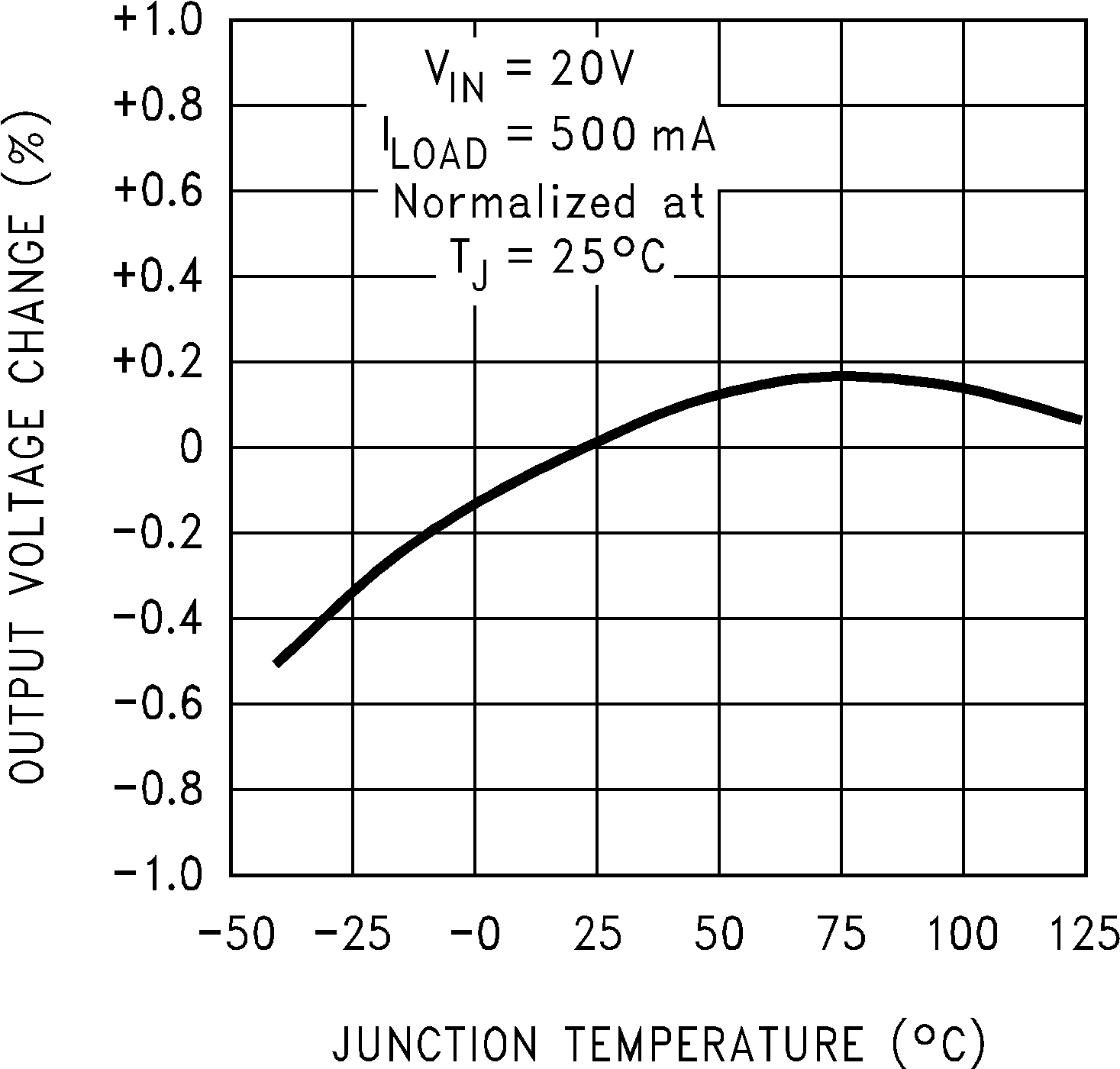
GUID-A87B10B4-09F9-43D1-91BB-18B975526F28-low.png
Figure 6-1 Normalized Output Voltage
GUID-53311BBD-AF08-427E-92A1-294E7546101A-low.png
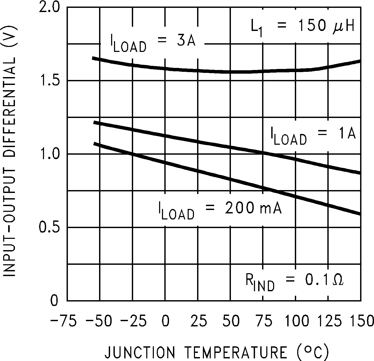
Figure 6-3 Dropout Voltage
GUID-8300F5A4-03F0-4CA8-BA74-D112B574A19D-low.png
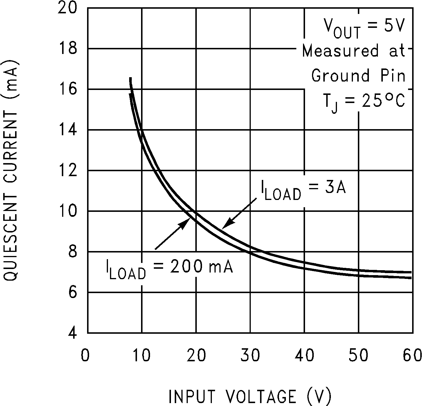
Figure 6-5 Quiescent Current
GUID-87748A88-66CB-4471-A8FD-D3E6E8229EC8-low.png
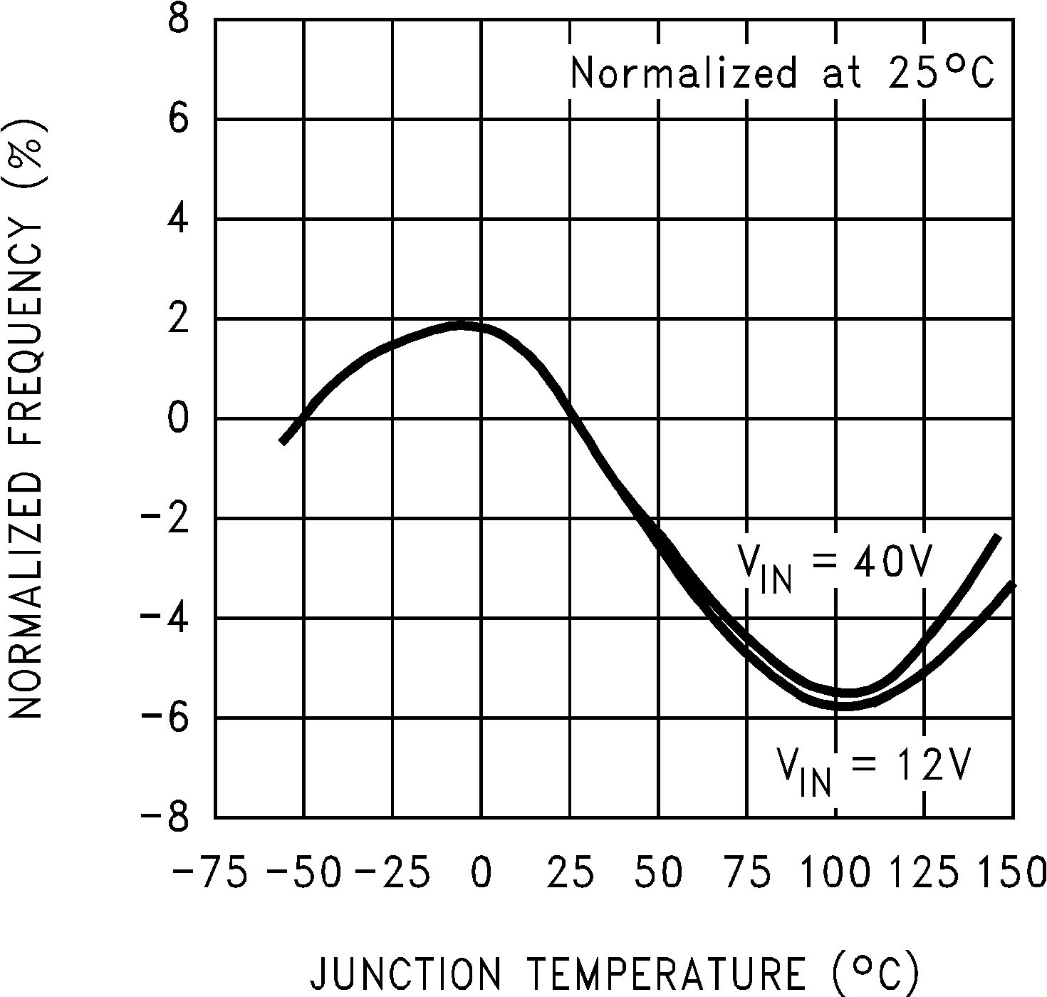
Figure 6-7 Oscillator Frequency
GUID-80A11A86-5680-4756-94B4-E7806052E52C-low.png
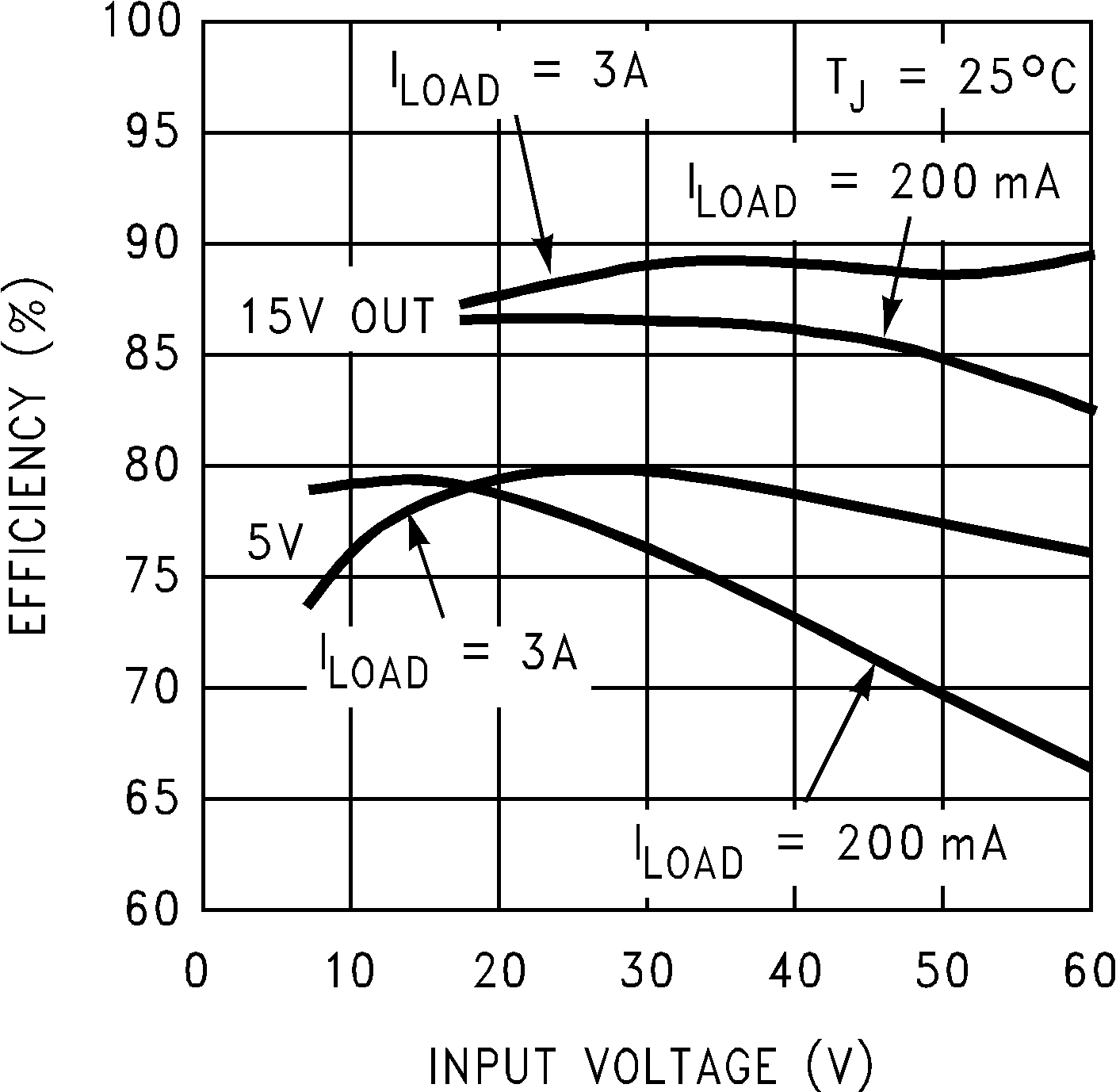
Figure 6-9 Efficiency
GUID-9A206636-6963-405C-93E0-BABB2F2DDF29-low.png
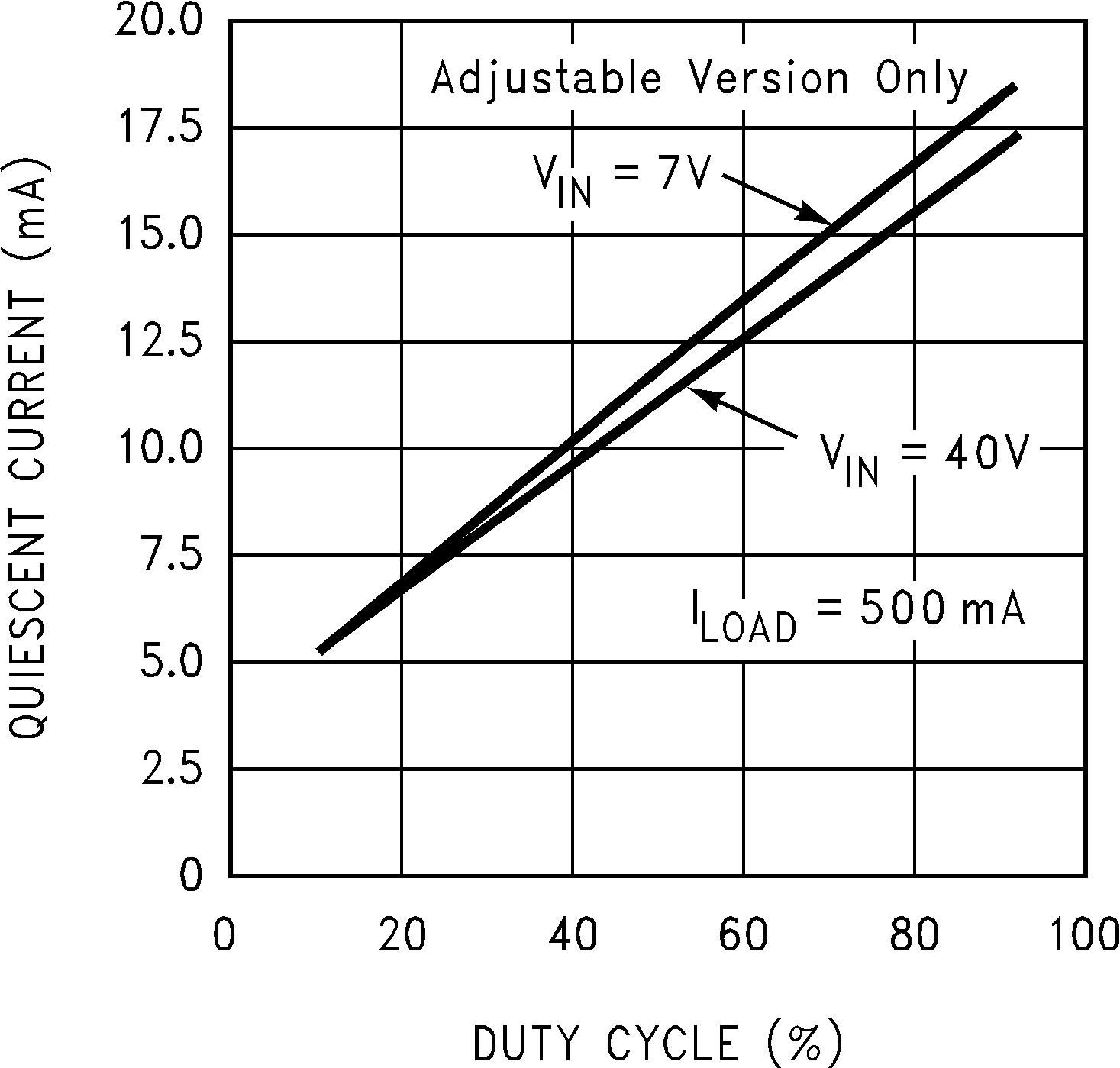
Figure 6-11 Quiescent Current vs Duty Cycle
GUID-502E3DB4-C814-491C-8B54-E769C839B07A-low.png
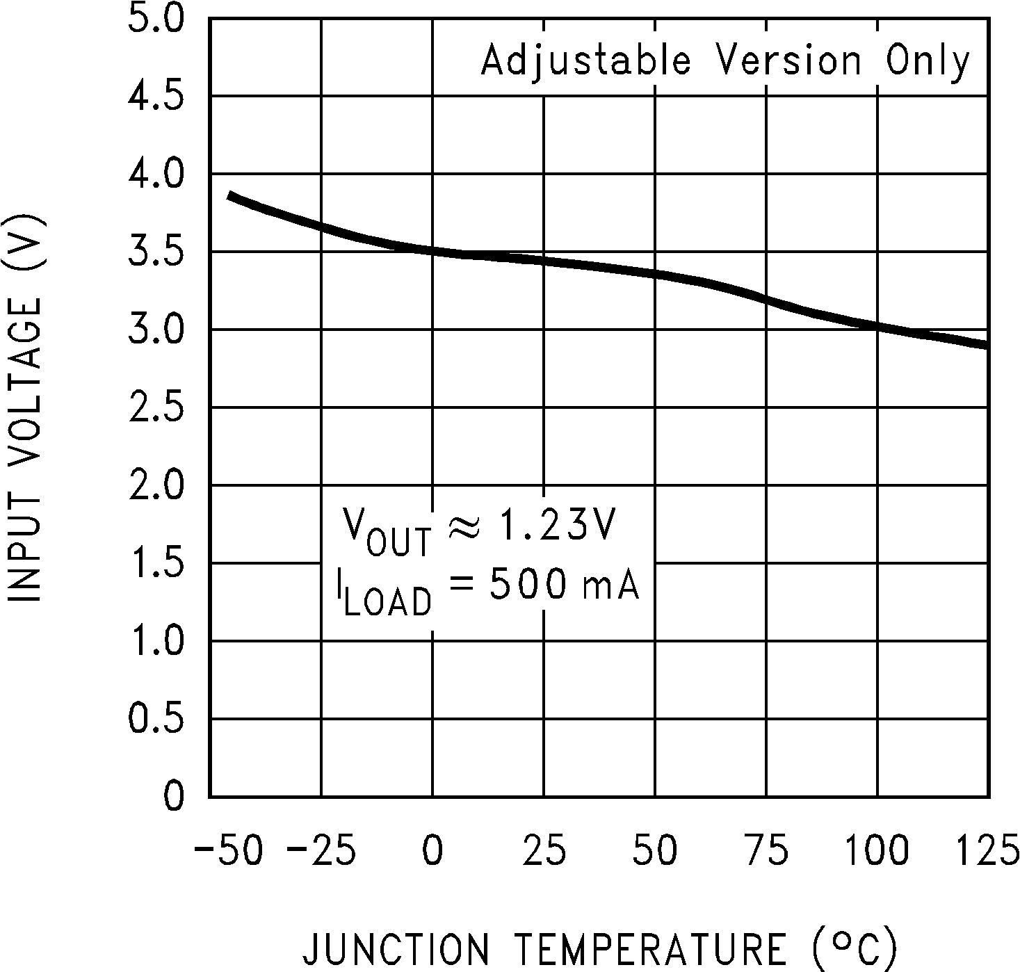
Figure 6-13 Minimum Operating Voltage
GUID-DBD00DD1-1E30-446D-8668-7999D3291666-low.png
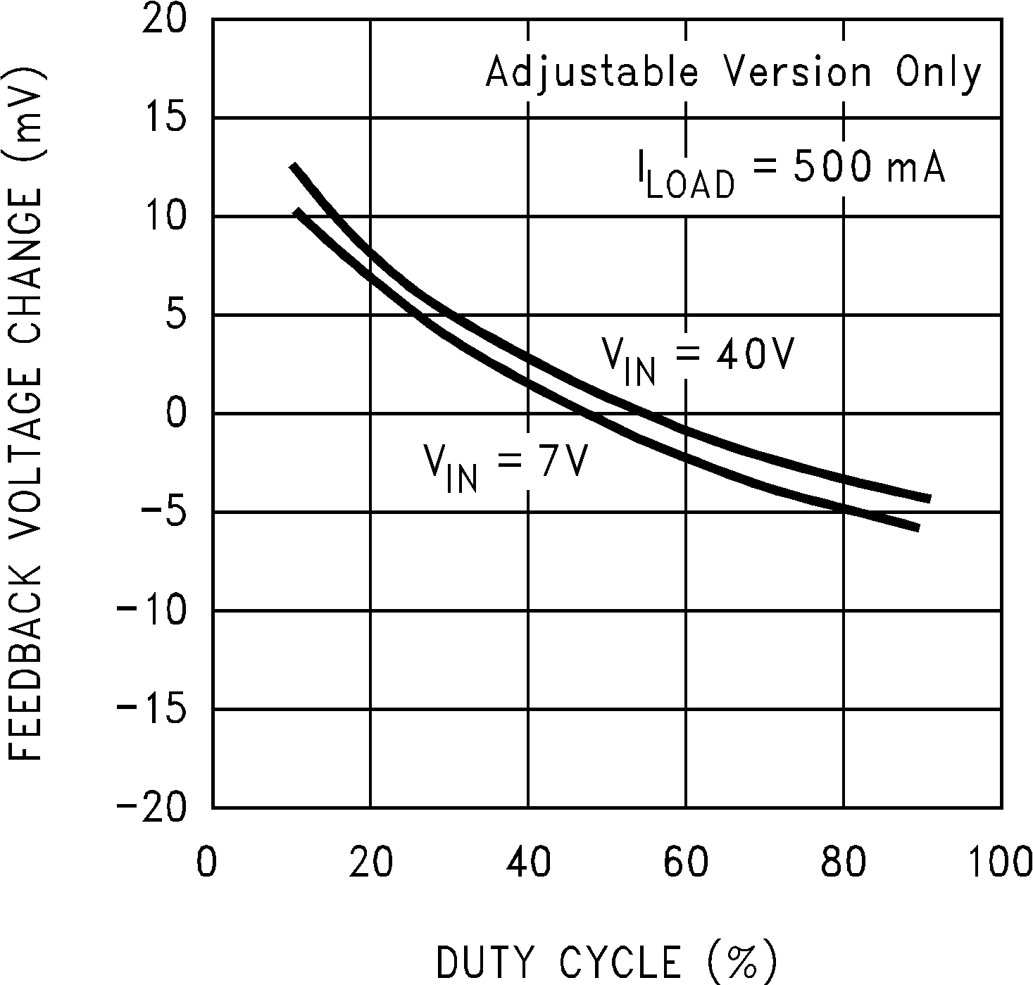
Figure 6-15 Feedback Voltage vs Duty Cycle
GUID-5EA62507-EDB9-487B-B394-6B1F2A39868C-low.png
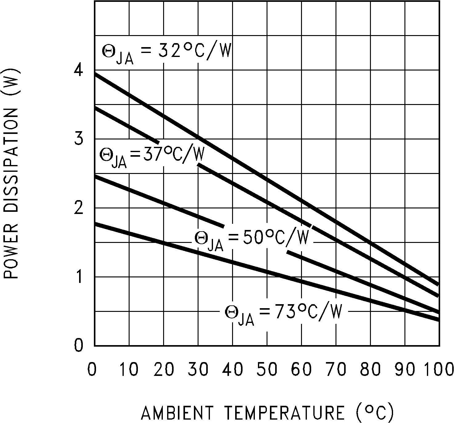
If the DDPAK/TO-263 package is used, the thermal resistance can be reduced by increasing the PCB copper area thermally connected to the package. Using 0.5 square inches of copper area, θJA is 50°C/W, with 1 square inch of copper area, θJA is 37°C/W, and with 1.6 or more square inches of copper area, θJA is 32°C/W.
Figure 6-17 Maximum Power Dissipation (DDPAK/TO-263)
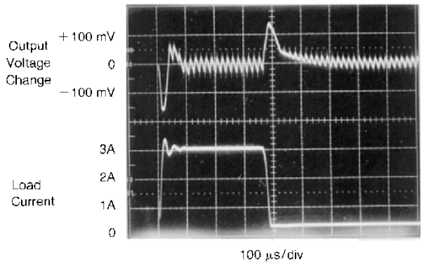
GUID-2F812FD1-888E-477A-AB2F-E5541D58AA96-low.gif
Figure 6-19 Load Transient Response
GUID-879D3B46-4727-4A3E-9E1F-B8CE8D99BA35-low.png
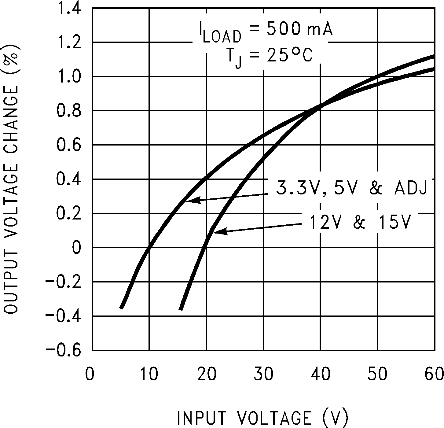
Figure 6-2 Line Regulation
GUID-C1BCA49D-CA91-42C9-95D1-C2C751AABCBC-low.png
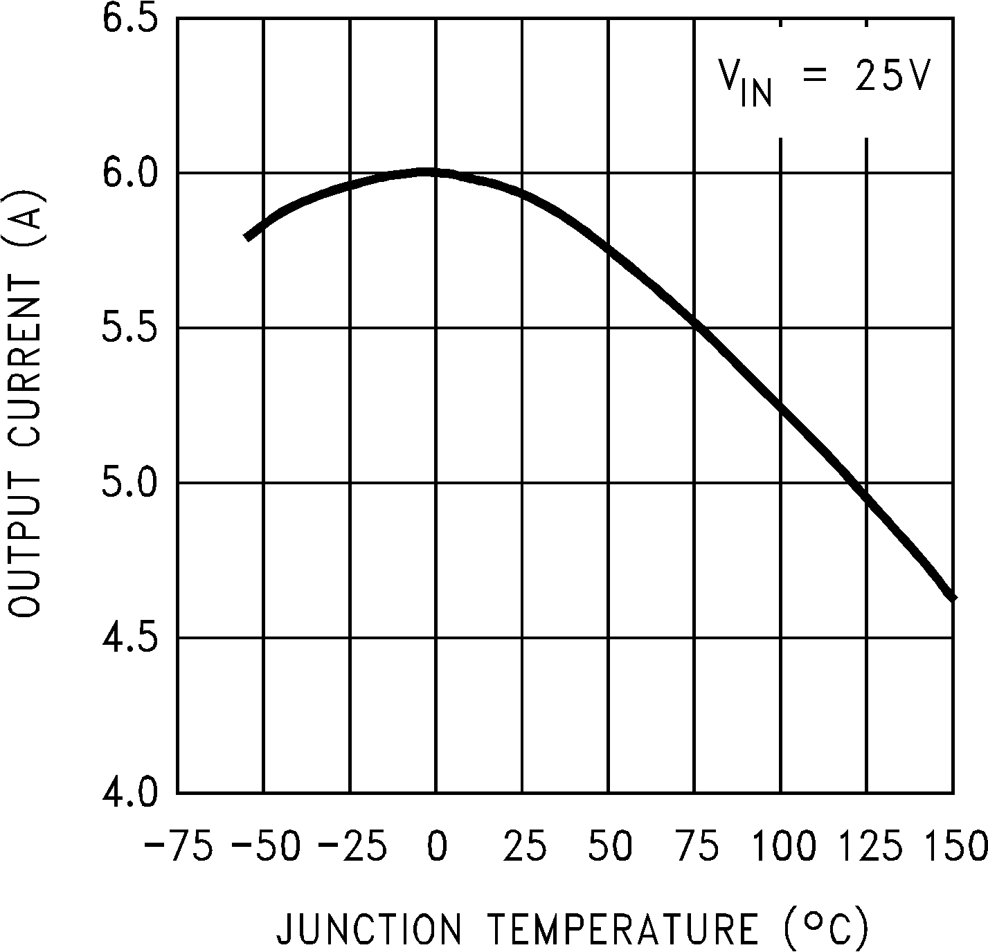
Figure 6-4 Current Limit
GUID-00CC72CE-BAD7-484D-83AE-2C37AB086AF2-low.png
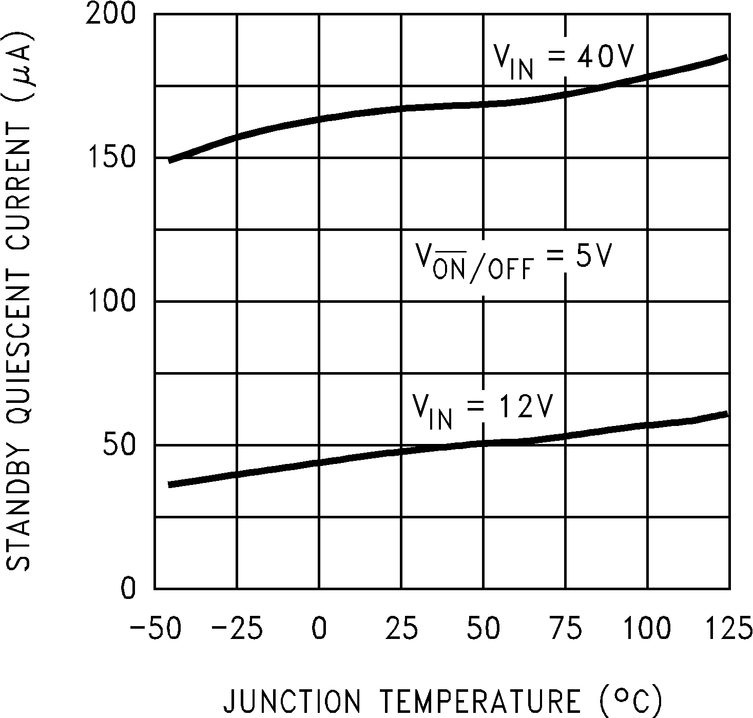
Figure 6-6 Standby Quiescent Current
GUID-CAB2B079-EDB5-4F62-9B1B-2A15E3103C33-low.png
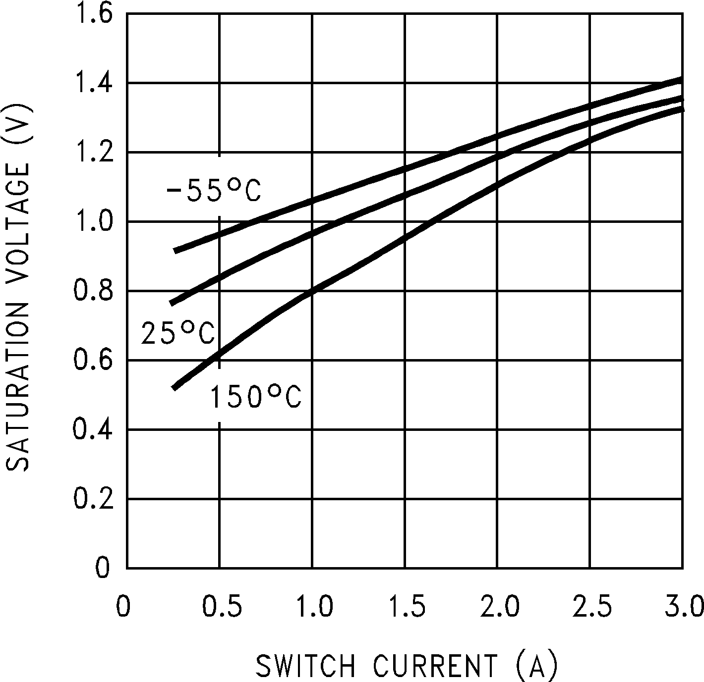
Figure 6-8 Switch Saturation Voltage
GUID-502E3DB4-C814-491C-8B54-E769C839B07A-low.png
Figure 6-10 Minimum Operating Voltage
GUID-DBD00DD1-1E30-446D-8668-7999D3291666-low.png
Figure 6-12 Feedback Voltage vs Duty Cycle
GUID-9A206636-6963-405C-93E0-BABB2F2DDF29-low.png
Figure 6-14 Quiescent Current vs Duty Cycle
GUID-A0D9D1F5-1AE1-4D60-8127-3DA09C52EAD1-low.png
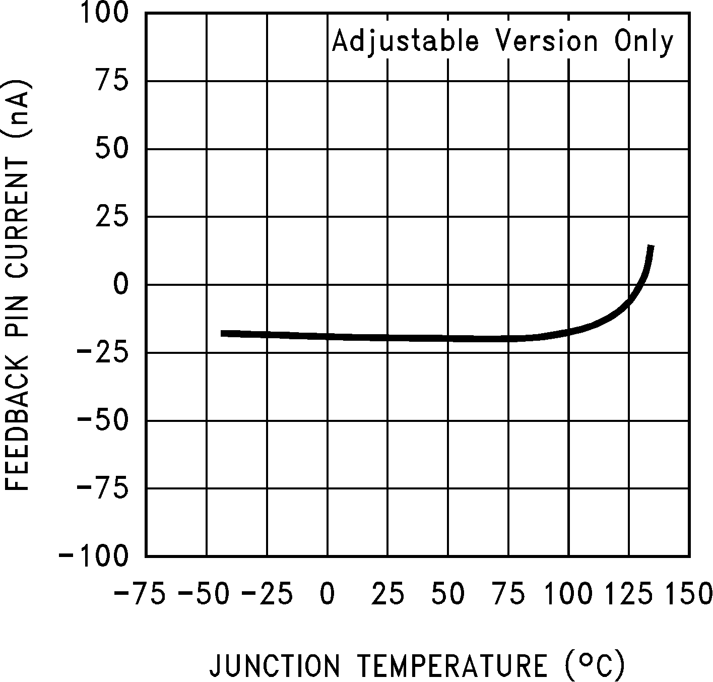
Figure 6-16 Feedback Pin Current
GUID-E7BB0F38-52D6-4A7F-861C-EBF437A640BA-low.png
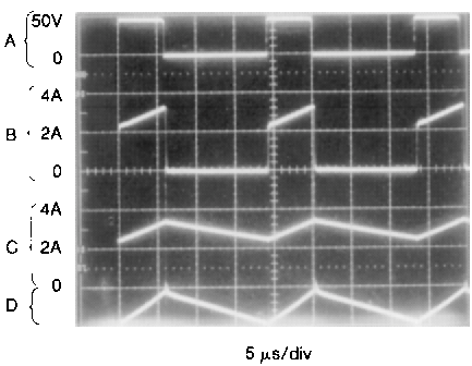
VOUT = 15 V A: Output Pin Voltage, 50 V/div B: Output Pin Current, 2 A/div C: Inductor Current, 2 A/div D: Output Ripple Voltage, 50 mV/div, AC-CoupledHorizontal Time Base: 5 μs/div
Figure 6-18 Switching Waveforms