SNVS074E May 2001 – May 2016 LM2591HV
PRODUCTION DATA.
- 1 Features
- 2 Applications
- 3 Description
- 4 Revision History
- 5 Description (continued)
- 6 Pin Configuration and Functions
-
7 Specifications
- 7.1 Absolute Maximum Ratings
- 7.2 ESD Ratings
- 7.3 Recommended Operating Conditions
- 7.4 Thermal Information
- 7.5 Electrical Characteristics LM2591HV-3.3
- 7.6 Electrical Characteristics LM2591HV-5.0
- 7.7 Electrical Characteristics LM2591HV-ADJ
- 7.8 Electrical Characteristics All Output Voltage Versions
- 7.9 Typical Characteristics
- 8 Parameter Measurement Information
- 9 Detailed Description
- 10Application and Implementation
- 11Power Supply Recommendations
- 12Layout
- 13Device and Documentation Support
- 14Mechanical, Packaging, and Orderable Information
Package Options
Mechanical Data (Package|Pins)
Thermal pad, mechanical data (Package|Pins)
- KTT|5
Orderable Information
7 Specifications
7.1 Absolute Maximum Ratings(1)(2)
| MIN | MAX | UNIT | |||
|---|---|---|---|---|---|
| Maximum supply voltage (VIN) | 63 | V | |||
| ON/OFF pin voltage | −0.3 | 25 | V | ||
| Feedback pin voltage | −0.3 | 25 | V | ||
| Output voltage to ground | (Steady-state) | −1 | V | ||
| Power dissipation | Internally limited | ||||
| Lead temperature | KTT package | Vapor phase (60 sec.) | 215 | °C | |
| Infrared (10 sec.) | 245 | ||||
| NDH package (Soldering, 10 sec.) | 260 | ||||
| Maximum junction temperature | 150 | °C | |||
| Storage temperature, Tstg | −65 | 150 | °C | ||
(1) Stresses beyond those listed under Absolute Maximum Ratings may cause permanent damage to the device. These are stress ratings only, which do not imply functional operation of the device at these or any other conditions beyond those indicated under Recommended Operating Conditions. Exposure to absolute-maximum-rated conditions for extended periods may affect device reliability.
(2) If Military/Aerospace specified devices are required, please contact the TI Sales Office/ Distributors for availability and specifications.
7.2 ESD Ratings
| VALUE | UNIT | |||
|---|---|---|---|---|
| V(ESD) | Electrostatic discharge | Human-body model (HBM), per ANSI/ESDA/JEDEC JS-001(1)(2) | ±2000 | V |
(1) JEDEC document JEP155 states that 500-V HBM allows safe manufacturing with a standard ESD control process.
(2) The human body model is a 100-pF capacitor discharged through a 1.5-kΩ resistor into each pin.
7.3 Recommended Operating Conditions
| MIN | MAX | UNIT | |
|---|---|---|---|
| Temperature | −40 | 125 | °C |
| Supply voltage | 4.5 | 60 | V |
7.4 Thermal Information
| THERMAL METRIC(1) | LM2591HV | UNIT | |||
|---|---|---|---|---|---|
| KTT (DDPAK/TO-263) | NDH (TO-220) | ||||
| 5 PINS | 5 PINS | ||||
| RθJA | Junction-to-ambient thermal resistance | See (2)(3) | 50 | 50 | °C/W |
| RθJC(top) | Junction-to-case (top) thermal resistance | 2 | 2 | °C/W | |
(1) For more information about traditional and new thermal metrics, see the Semiconductor and IC Package Thermal Metrics application report, SPRA953.
(2) The package thermal impedance is calculated in accordance to JESD 51-7
(3) Thermal Resistances were simulated on a 4-layer, JEDEC board
7.5 Electrical Characteristics LM2591HV-3.3
Specifications are for TJ = 25°C unless otherwise noted.| PARAMETER | TEST CONDITIONS | MIN(1) | TYP(2) | MAX(1) | UNIT | ||
|---|---|---|---|---|---|---|---|
| SYSTEM PARAMETERS – See Test Circuits(3) | |||||||
| VOUT | Output Voltage | 4.75 V ≤ VIN ≤ 60 V, 0.2 A ≤ ILOAD ≤ 1 A |
3.168 | 3.3 | 3.432 | V | |
| TA = –40°C to 125°C | 3.135 | 3.465 | |||||
| η | Efficiency | VIN = 12 V, ILOAD = 1 A | 77% | ||||
(1) All limits ensured at room temperature (TJ = 25°C) unless otherwise noted. All room temperature limits are 100% production tested. All limits at temperature extremes are ensured through correlation using standard Statistical Quality Control (SQC) methods. All limits are used to calculate Average Outgoing Quality Level (AOQL).
(2) Typical numbers are at 25°C and represent the most likely norm.
(3) External components such as the catch diode, inductor, input and output capacitors can affect switching regulator system performance. When the LM2591HV is used as shown in Test Circuits test circuit, system performance will be as shown in Electrical Characteristics.
7.6 Electrical Characteristics LM2591HV-5.0
Specifications are for TJ = 25°C unless otherwise noted.| PARAMETER | TEST CONDITIONS | MIN(1) | TYP(2) | MAX(1) | UNIT | ||
|---|---|---|---|---|---|---|---|
| SYSTEM PARAMETERS – See Test Circuits(3) | |||||||
| VOUT | Output Voltage | 7 V ≤ VIN ≤ 60 V, 0.2 A ≤ ILOAD ≤ 1 A | 4.8 | 5 | 5.2 | V | |
| TA = –40°C to 125°C | 4.75 | 5.25 | |||||
| η | Efficiency | VIN = 12 V, ILOAD = 1 A | 82% | ||||
(1) All limits ensured at room temperature (TJ = 25°C) unless otherwise noted. All room temperature limits are 100% production tested. All limits at temperature extremes are ensured through correlation using standard Statistical Quality Control (SQC) methods. All limits are used to calculate Average Outgoing Quality Level (AOQL).
(2) Typical numbers are at 25°C and represent the most likely norm.
(3) External components such as the catch diode, inductor, input and output capacitors can affect switching regulator system performance. When the LM2591HV is used as shown in Test Circuits test circuit, system performance will be as shown in Electrical Characteristics.
7.7 Electrical Characteristics LM2591HV-ADJ
Specifications are for TJ = 25°C unless otherwise noted| PARAMETER | TEST CONDITIONS | MIN(1) | TYP(2) | MAX(1) | UNIT | ||
|---|---|---|---|---|---|---|---|
| SYSTEM PARAMETERS – See Test Circuits(3) | |||||||
| VFB | Feedback Voltage | 4.5 V ≤ VIN ≤ 60 V, 0.2 A ≤ ILOAD ≤ 1 A VOUT programmed for 3 V. Circuit of Test Circuits. |
1.193 | 1.23 | 1.267 | V | |
| TA = –40°C to 125°C | 1.18 | 1.28 | |||||
| η | Efficiency | VIN = 12 V, VOUT = 3 V, ILOAD = 1 A | 76% | ||||
(1) All limits ensured at room temperature (TJ = 25°C) unless otherwise noted. All room temperature limits are 100% production tested. All limits at temperature extremes are ensured through correlation using standard Statistical Quality Control (SQC) methods. All limits are used to calculate Average Outgoing Quality Level (AOQL).
(2) Typical numbers are at 25°C and represent the most likely norm.
(3) External components such as the catch diode, inductor, input and output capacitors can affect switching regulator system performance. When the LM2591HV is used as shown in Test Circuits test circuit, system performance will be as shown in Electrical Characteristics.
7.8 Electrical Characteristics All Output Voltage Versions
Specifications are for TJ = 25°C, ILOAD = 500 mA, and VIN = 12V for the 3.3-V, 5-V, and adjustable versions, unless otherwise noted.| PARAMETER | TEST CONDITIONS | MIN(1) | TYP(2) | MAX(1) | UNIT | ||
|---|---|---|---|---|---|---|---|
| DEVICE PARAMETERS | |||||||
| Ib | Feedback Bias Current | Adjustable Version Only, VFB = 1.3 V | 10 | 50 | nA | ||
| TA = –40°C to 125°C | 100 | ||||||
| fO | Oscillator Frequency | See (3) | 127 | 150 | 173 | kHz | |
| TA = –40°C to 125°C | 110 | 173 | |||||
| VSAT | Saturation Voltage | IOUT = 1 A (4)(5) | 0.95 | 1.2 | V | ||
| TA = –40°C to 125°C | 1.3 | ||||||
| DC | Max Duty Cycle (ON) | See (5)(6) | 100% | ||||
| Min Duty Cycle (OFF) | 0% | ||||||
| ICLIM | Switch current Limit | Peak Current(4)(5) | 1.3 | 1.9 | 2.8 | A | |
| TA = –40°C to 125°C | 1.2 | 3.0 | |||||
| IL | Output Leakage Current | Output = 0 V | 5 | 50 | μA | ||
| Output = −1 V (4)(6)(7) | 5 | 30 | mA | ||||
| IQ | Operating Quiescent Current | SD/SS Pin Open (6) | 5 | 10 | mA | ||
| ISTBY | Standby Quiescent Current | SD/SS pin = 0 V (7) | 90 | 200 | μA | ||
| TA = –40°C to 125°C | 250 | ||||||
| ON/OFF CONTROL – See Test Circuits | |||||||
| VIH
VIL |
ON/OFF Pin Logic Input Threshold Voltage | Low (Regulator ON) High (Regulator OFF) |
1.3 | V | |||
| TA = –40°C to 125°C | 2.0 | 0.6 | |||||
| IH | ON/OFF Pin Input Current | VLOGIC = 2.5 V (Regulator OFF) | 5 | 15 | μA | ||
| IL | VLOGIC = 0.5 V (Regulator ON) | 0.02 | 5 | μA | |||
(1) All limits ensured at room temperature (TJ = 25°C) unless otherwise noted. All room temperature limits are 100% production tested. All limits at temperature extremes are ensured through correlation using standard Statistical Quality Control (SQC) methods. All limits are used to calculate Average Outgoing Quality Level (AOQL).
(2) Typical numbers are at 25°C and represent the most likely norm.
(3) The switching frequency is reduced when the second stage current limit is activated. The amount of reduction is determined by the severity of current overload.
(4) No diode, inductor or capacitor connected to output pin.
(5) Feedback pin removed from output and connected to 0 V to force the output transistor switch ON.
(6) Feedback pin removed from output and connected to 12 V for the 3.3-V, 5-V, and the ADJ. version to force the output transistor switch OFF.
(7) VIN = 60 V.
7.9 Typical Characteristics
(Circuit of Test Circuits)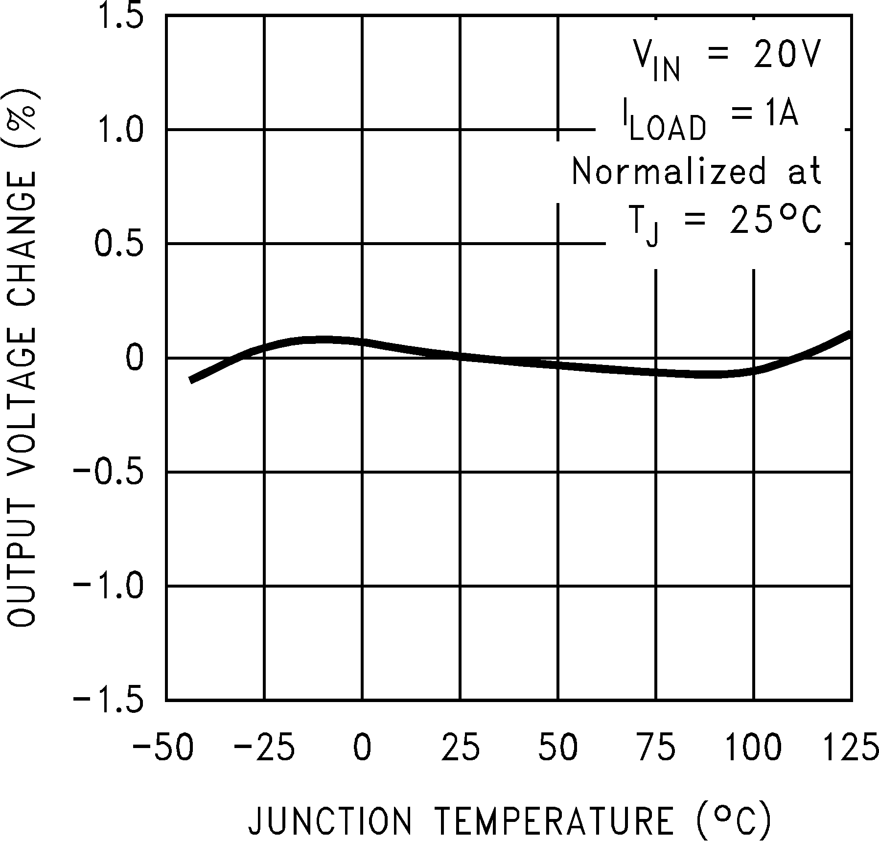 Figure 1. Normalized Output Voltage
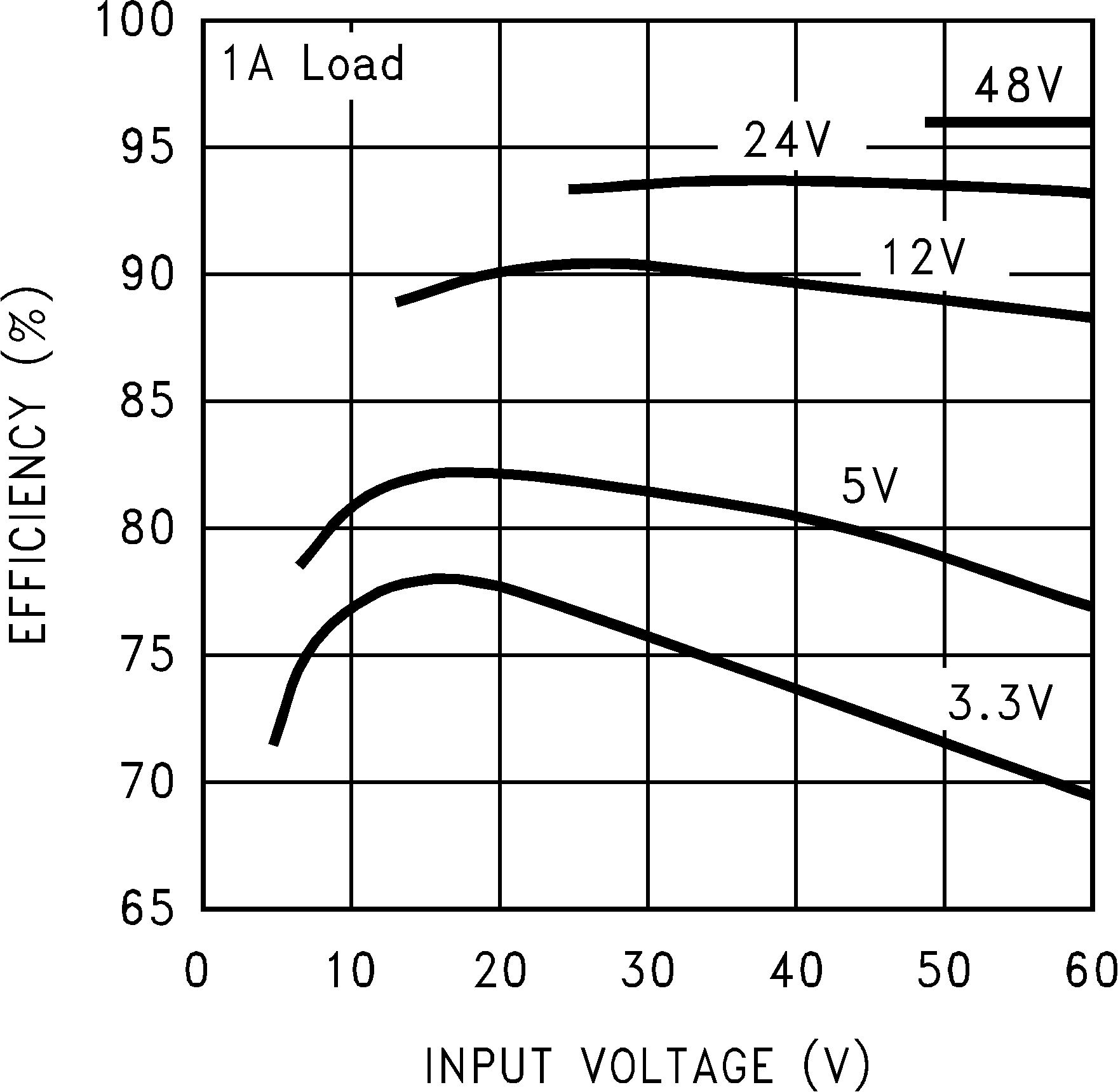 Figure 3. Efficiency
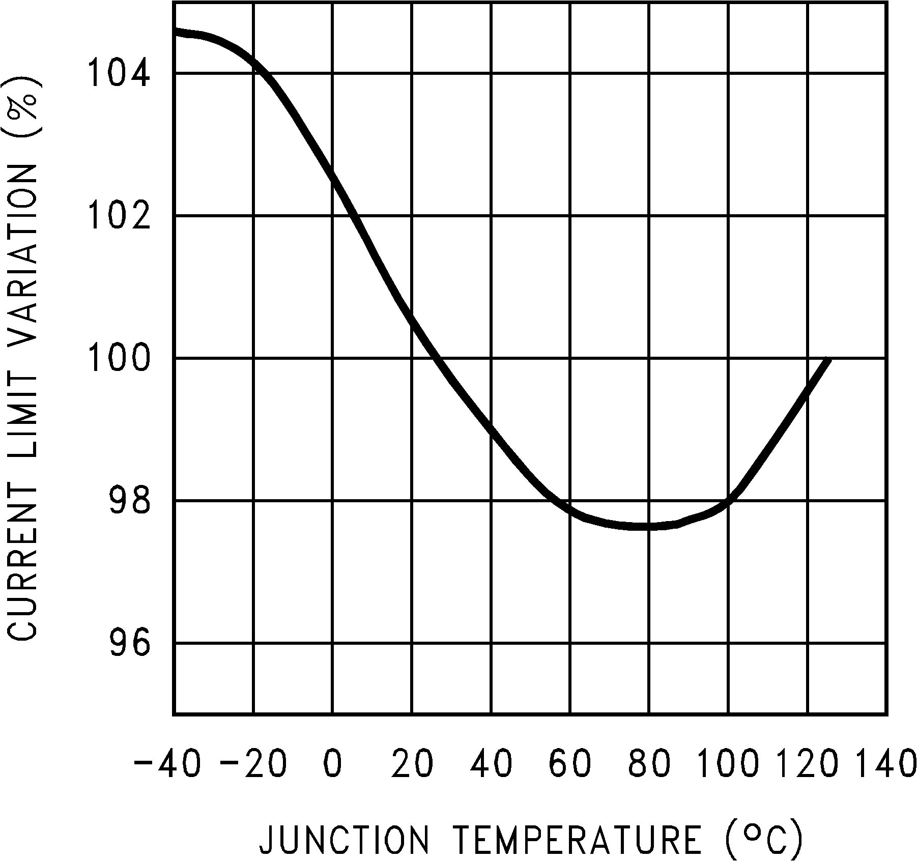 Figure 5. Switch Current Limit
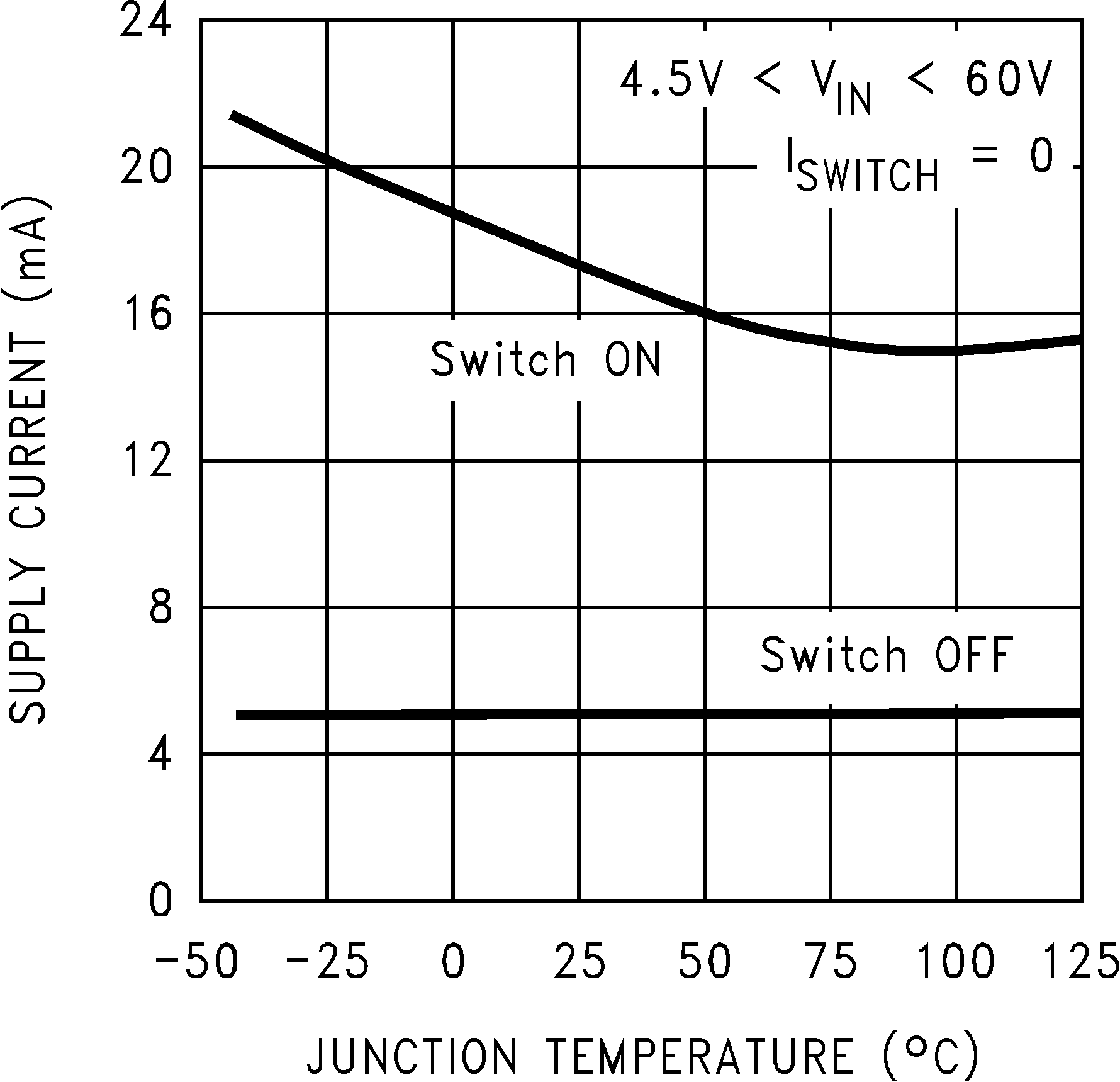 Figure 7. Operating Quiescent Current
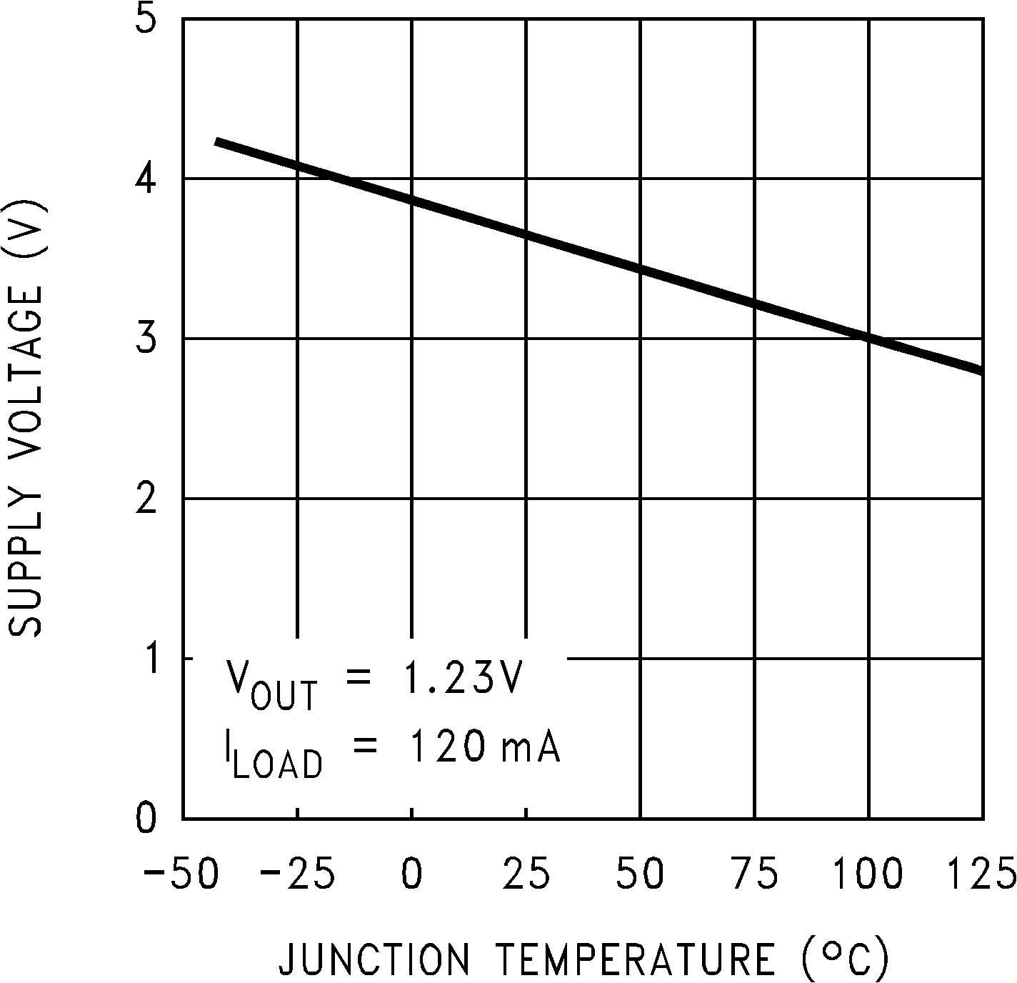 Figure 9. Minimum Operating Supply Voltage
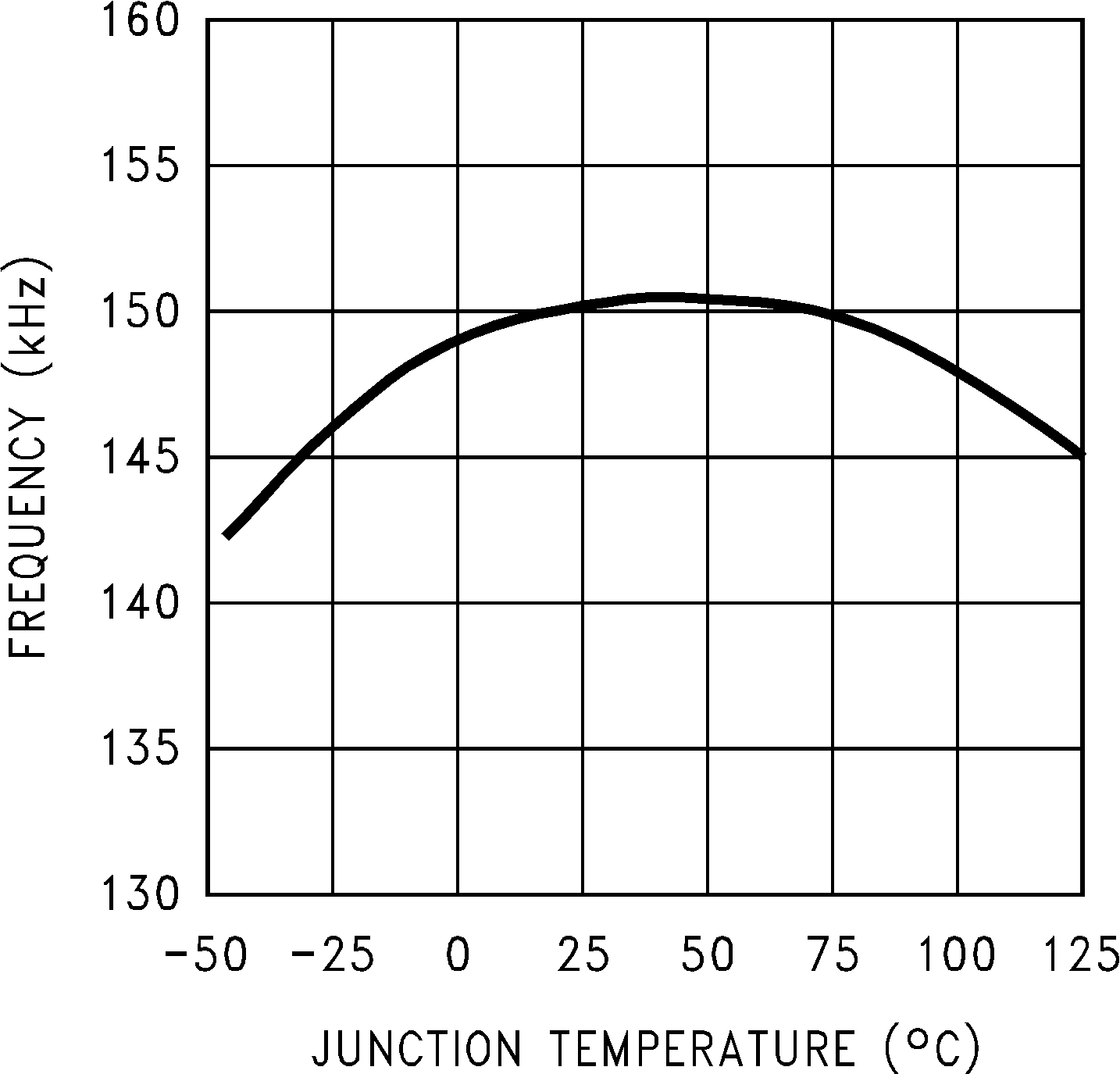 Figure 11. Switching Frequency
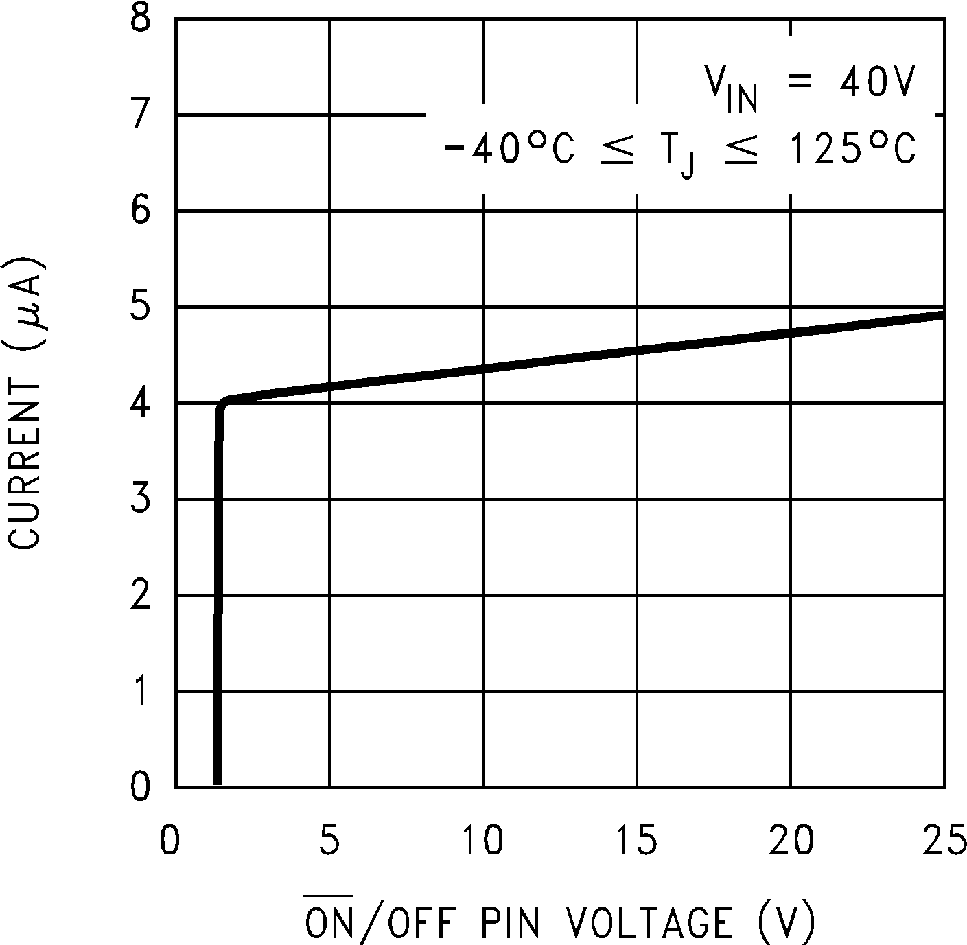
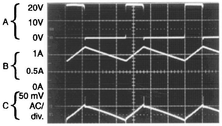
| Continuous Mode Switching Waveforms VIN = 20V, VOUT = 5V, ILOAD = 1A L = 52 μH, COUT = 100 μF, COUT ESR = 100 mΩ | ||
| Output Pin Voltage, 10V/div. | ||
| Inductor Current 0.5A/div. | ||
| Output Ripple Voltage, 50 mV/div. |
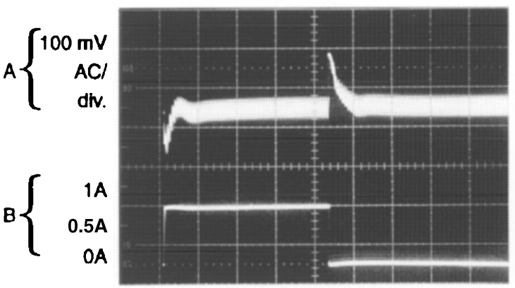
| Load Transient Response for Continuous Mode VIN = 20V, VOUT = 5V, ILOAD = 250 mA to 1A L = 52 μH, COUT = 100 μF, COUT ESR = 100 mΩ | ||
| Output Voltage, 100 mV/div. (AC) | ||
| 250 mA to 1A Load Pulse |
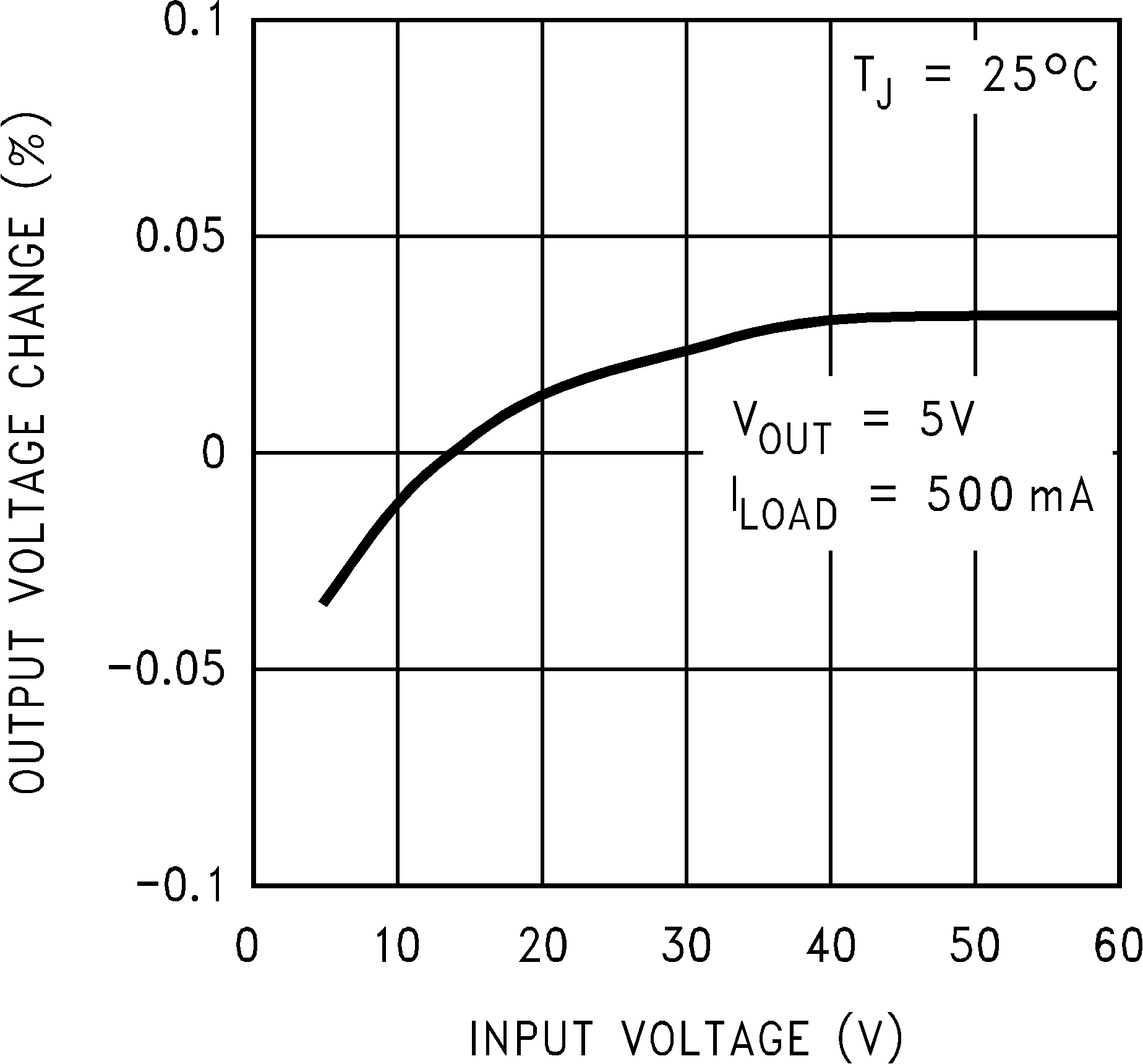 Figure 2. Line Regulation
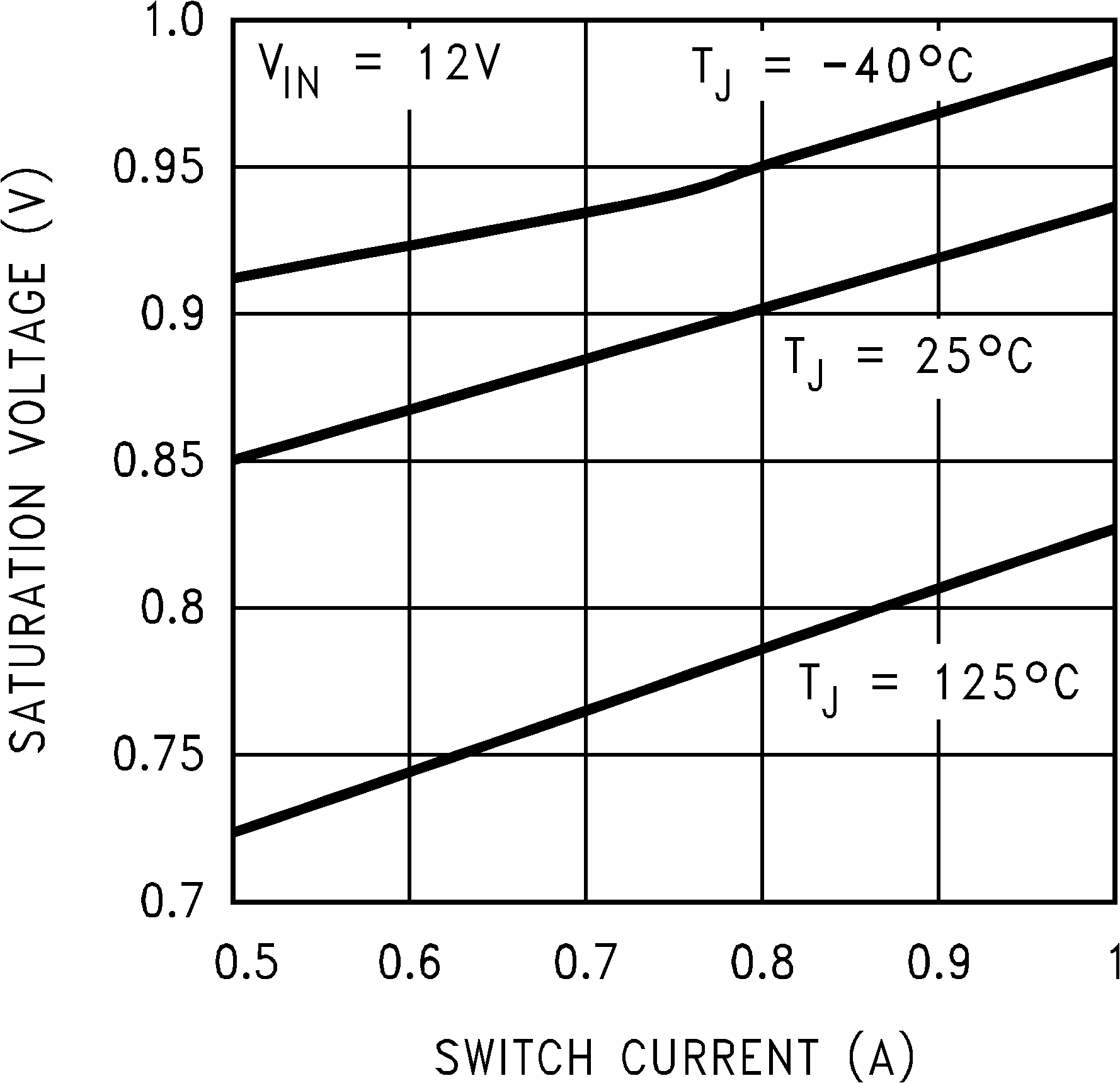 Figure 4. Switch Saturation Voltage
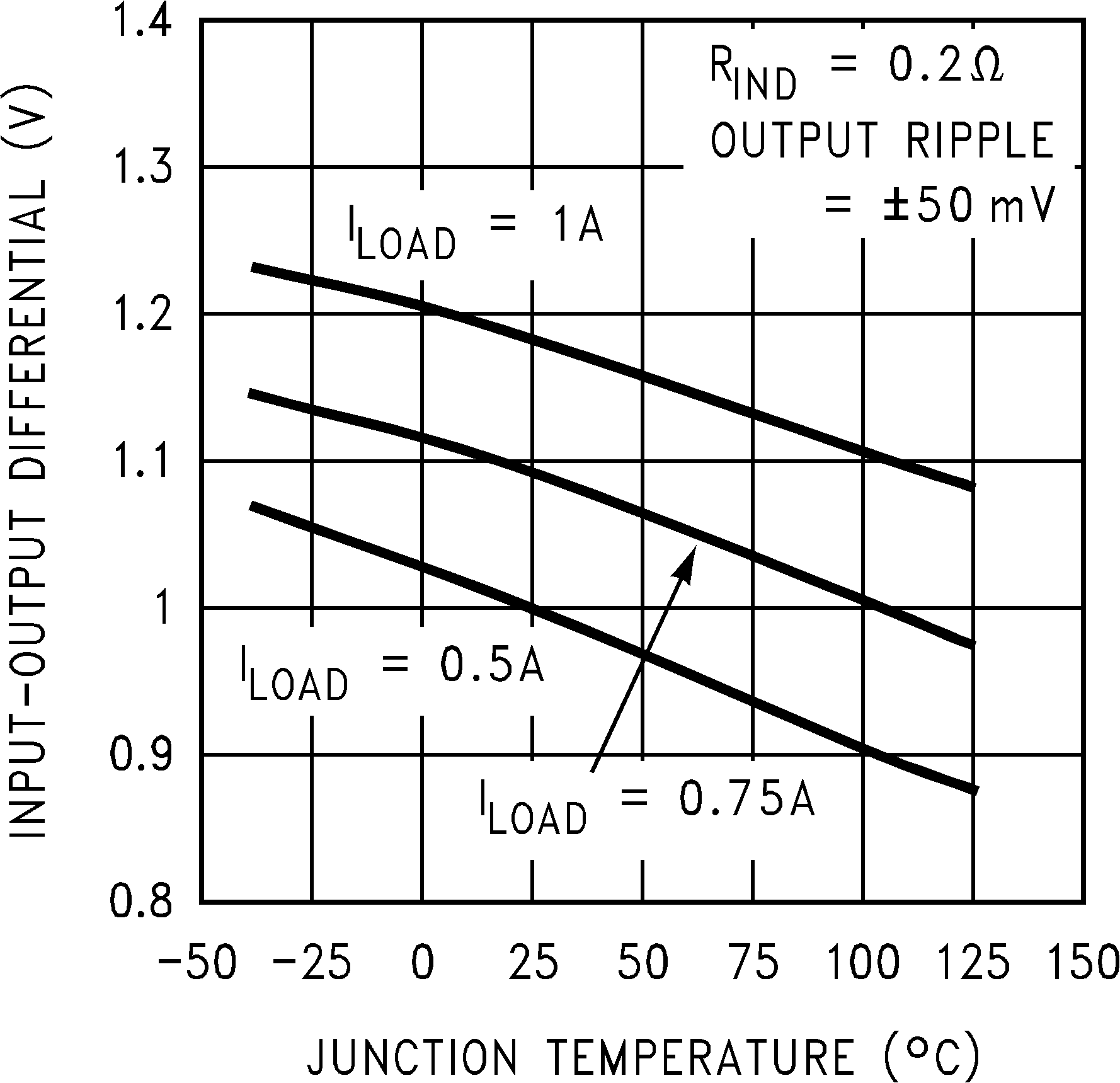 Figure 6. Dropout Voltage
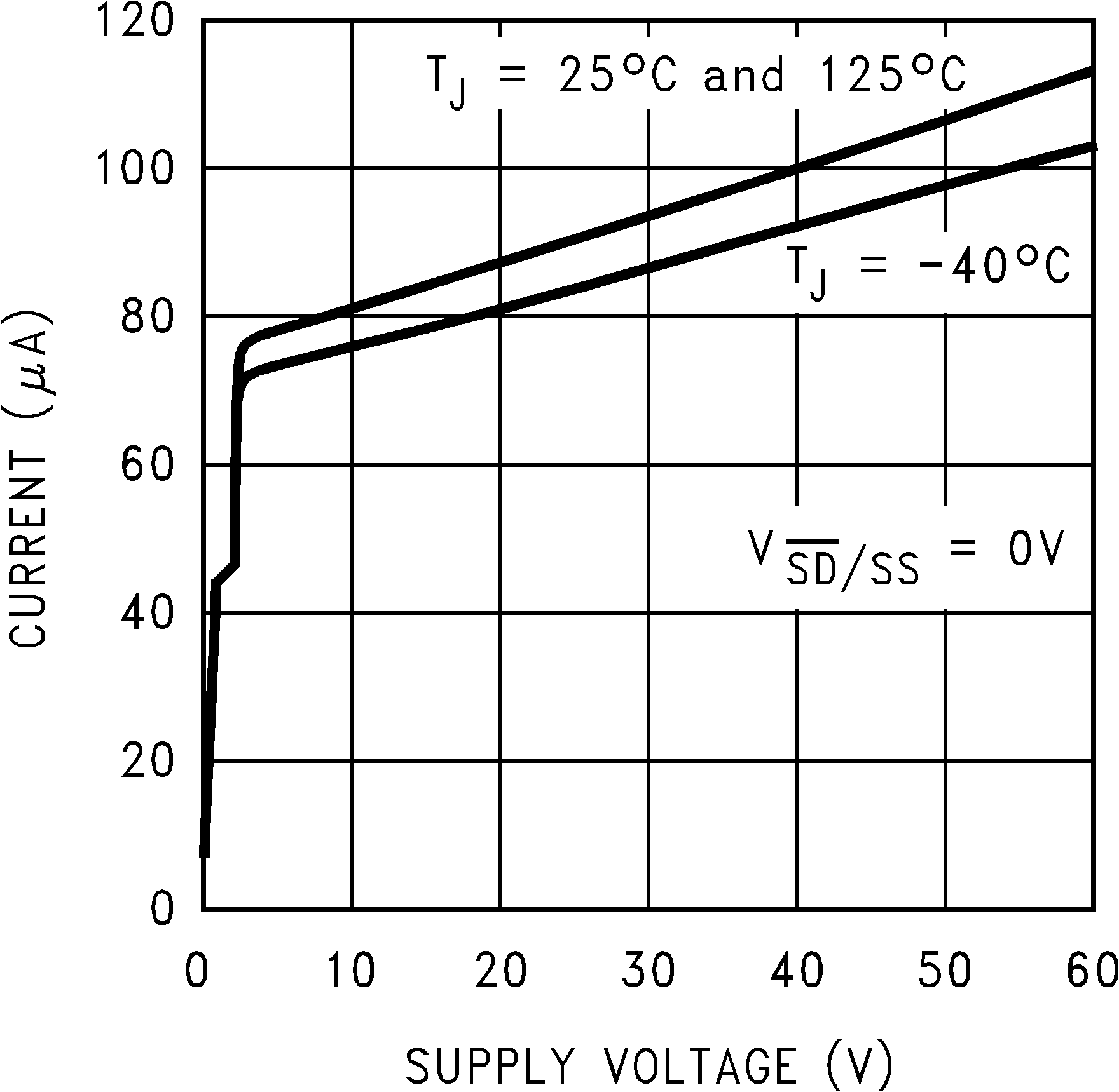 Figure 8. Shutdown Quiescent Current
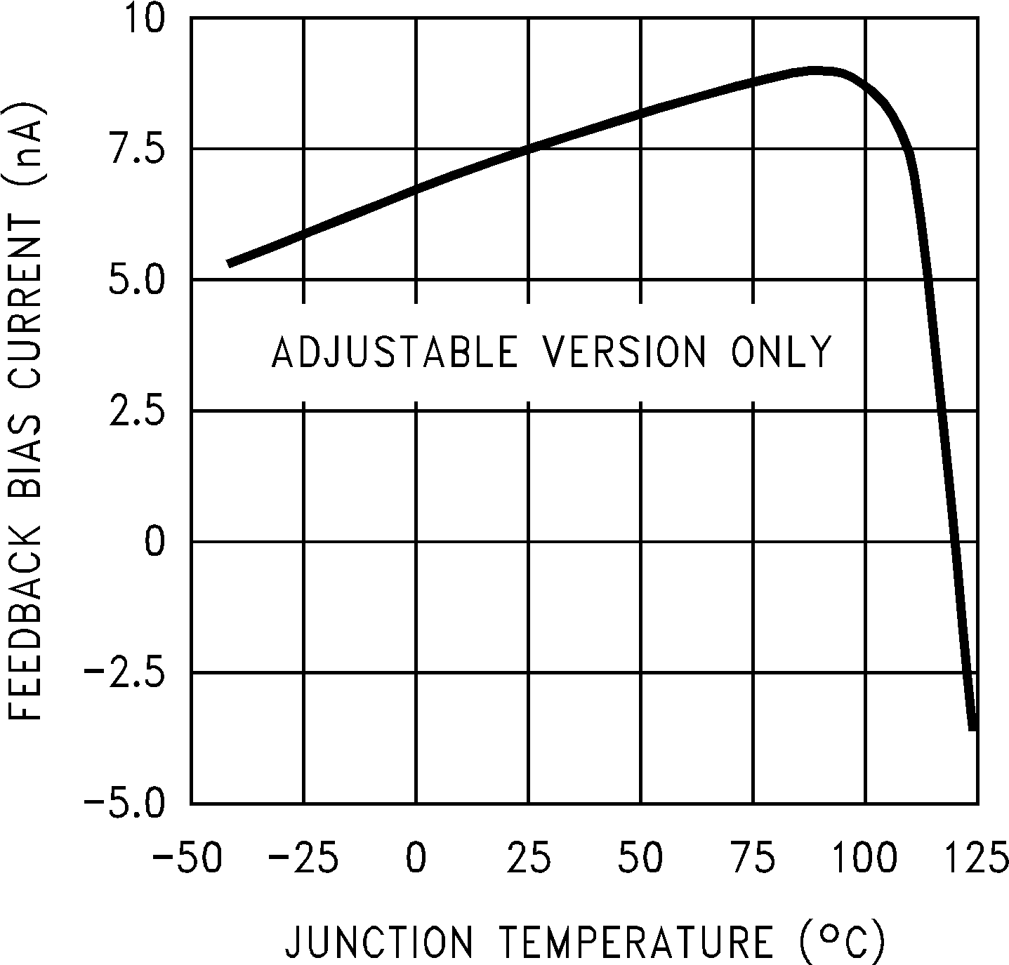 Figure 10. Feedback Pin Bias Current
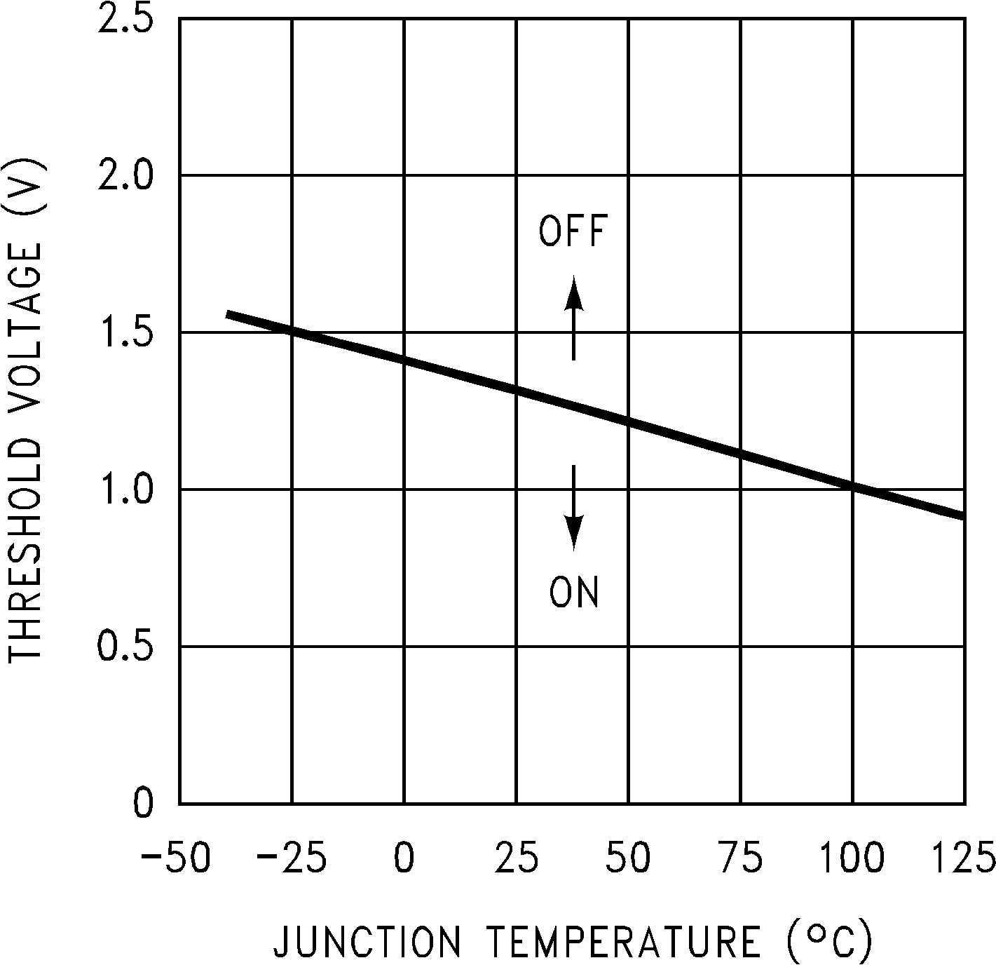 Figure 12. ON/OFF Threshold Voltage
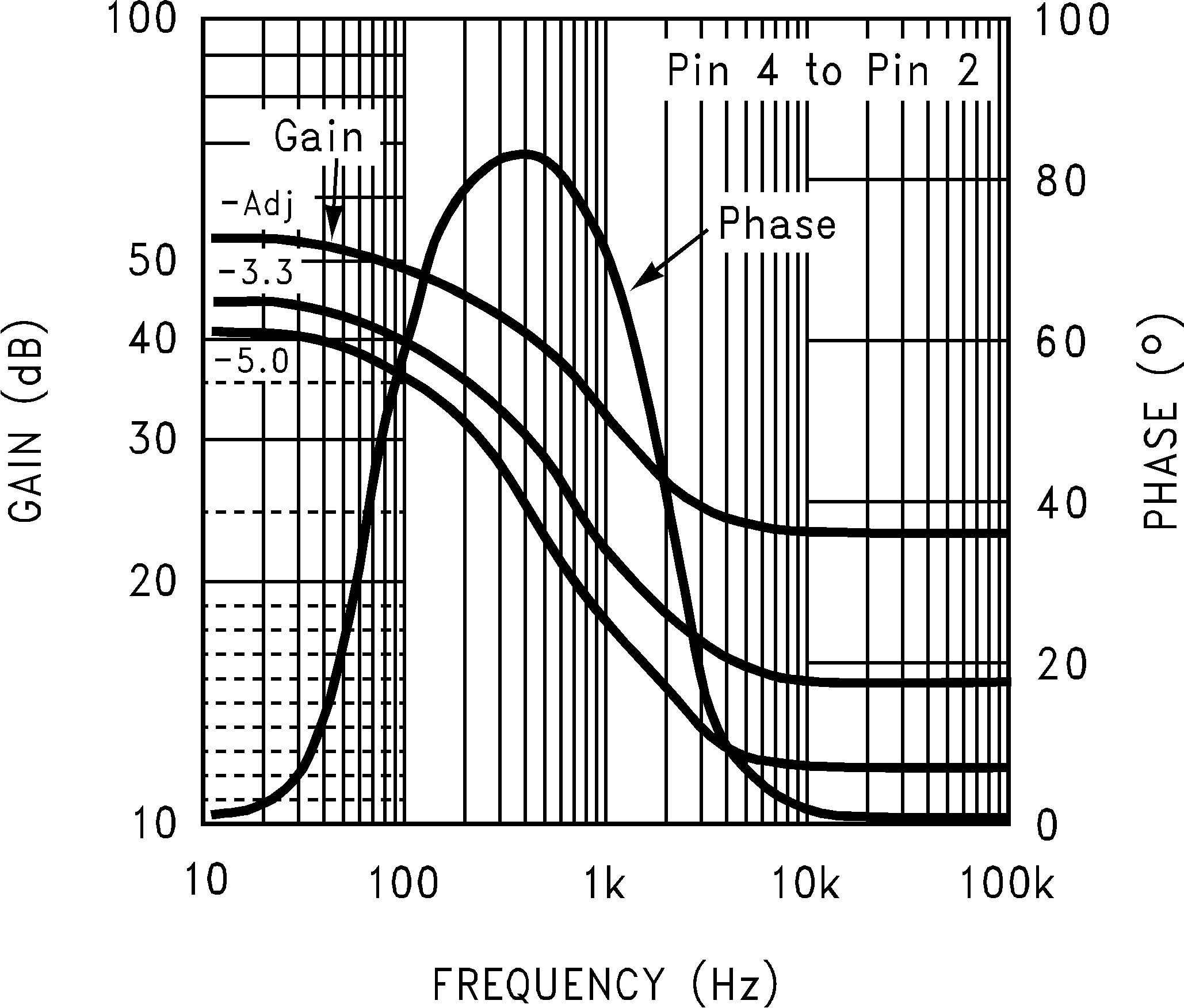 Figure 14. Internal Gain-Phase Characteristics
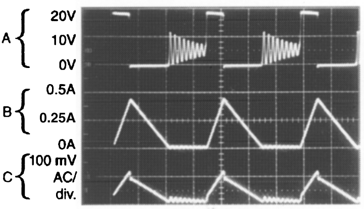
| Discontinuous Mode Switching Waveforms VIN = 20V, VOUT = 5V, ILOAD = 250 mA L = 15 μH, COUT = 150 μF, COUT ESR = 90 mΩ | ||
| Output Pin Voltage, 10V/div. | ||
| Inductor Current 0.25A/div. | ||
| Output Ripple Voltage, 100 mV/div. |
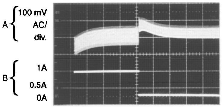
| Load Transient Response for Discontinuous Mode VIN = 20V, VOUT = 5V, ILOAD = 250 mA to 1A L = 15 μH, COUT = 150 μF, COUT ESR = 90 mΩ | ||
| Output Voltage, 100 mV/div. (AC) | ||
| 250 mA to 1A Load Pulse | ||