SNVS191F November 2002 – October 2016 LM2705
PRODUCTION DATA.
- 1 Features
- 2 Applications
- 3 Description
- 4 Revision History
- 5 Pin Configuration and Functions
- 6 Specifications
- 7 Detailed Description
- 8 Application and Implementation
- 9 Power Supply Recommendations
- 10Layout
- 11Device and Documentation Support
- 12Mechanical, Packaging, and Orderable Information
Package Options
Mechanical Data (Package|Pins)
- DBV|5
Thermal pad, mechanical data (Package|Pins)
Orderable Information
7 Detailed Description
7.1 Overview
The LM2705 is a small boost converter utilizing a constant off time architecture. The device can provide up to 20.5 V at the output with up to 150 mA of peak switch current.
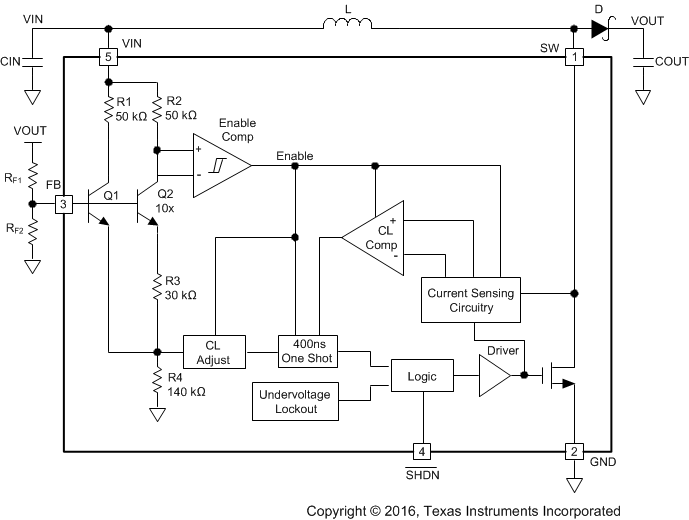
7.2 Functional Block Diagram

7.3 Feature Description
The LM2705 device features a constant off-time control scheme. Operation can be best understood by referring to Functional Block Diagram and Figure 11. Transistors Q1 and Q2 and resistors R3 and R4 of Functional Block Diagram form a bandgap reference used to control the output voltage. When the voltage at the FB pin is less than 1.237 V, the Enable Comp in Functional Block Diagram enables the device, and the NMOS switch is turned on pulling the SW pin to ground. When the NMOS switch is on, current begins to flow through inductor L while the load current is supplied by the output capacitor COUT. Once the current in the inductor reaches the current limit, the CL comp trips, and the 400-ns one shot turns off the NMOS switch.The SW voltage then rises to the output voltage plus a diode drop, and the inductor current begins to decrease as shown in Figure 11. During this time the energy stored in the inductor is transferred to COUT and the load. After the 400-ns off-time the NMOS switch is turned on, and energy is stored in the inductor again. This energy transfer from the inductor to the output causes a stepping effect in the output ripple as shown in Figure 11.
This cycle is continued until the voltage at FB reaches 1.237 V. When FB reaches this voltage, the Enable Comp disables the device, turning off the NMOS switch and reducing the IQ of the device to 40 µA. The load current is then supplied solely by COUT indicated by the gradually decreasing slope at the output as shown in Figure 11. When the FB pin drops slightly below 1.237 V, the Enable Comp enables the device and begins the cycle described previously.
7.4 Device Functional Modes
The SHDN pin can be used to turn off the LM2705 and reduce the IQ to 0.01 µA. In shutdown mode the output voltage is a diode drop lower than the input voltage.