SNVS100F March 2000 – July 2014 LM2937
PRODUCTION DATA.
- 1 Features
- 2 Applications
- 3 Description
- 4 Revision History
- 5 Pin Configuration and Functions
-
6 Specifications
- 6.1 Absolute Maximum Ratings
- 6.2 Handling Ratings
- 6.3 Recommended Operating Conditions
- 6.4 Thermal Information
- 6.5 Electrical Characteristics: LM2937-5
- 6.6 Electrical Characteristics: LM2937-8
- 6.7 Electrical Characteristics: LM2937-10
- 6.8 Electrical Characteristics: LM2937-12
- 6.9 Electrical Characteristics: LM2937-15
- 6.10 Typical Characteristics
- 7 Detailed Description
- 8 Application and Implementation
- 9 Power Supply Recommendations
- 10Layout
- 11Device and Documentation Support
- 12Mechanical, Packaging, and Orderable Information
Package Options
Mechanical Data (Package|Pins)
Thermal pad, mechanical data (Package|Pins)
Orderable Information
8 Application and Implementation
8.1 Application Information
Figure 18 shows the typical application circuit for the LM2937. The output capacitor, COUT, must have a capacitance value of at least 10 µF with an ESR of at least 10 mΩ, but no more than 3 Ω. The minimum capacitance value, and the ESR requirements apply across the entire expected operating ambient temperature range.
8.2 Typical Application
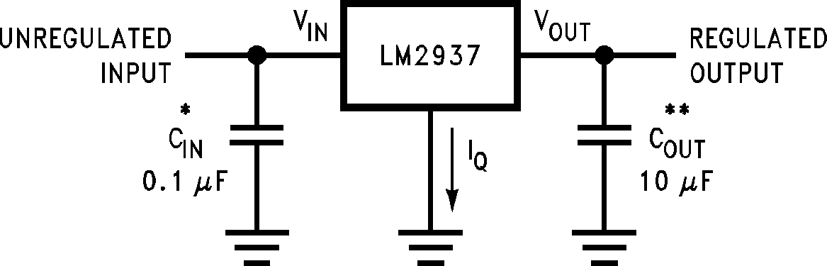 Figure 18. LM2937 Typical Application
| *Required if the regulator is located more than 3 inches from the power-supply-filter capacitors. | ||
| **Required for stability. COUT must be at least 10 µF (over full expected operating temperature range) and located as close as possible to the regulator. The equivalent series resistance, ESR, of this capacitor may be as high as 3 Ω. | ||
8.2.1 Design Requirements
For this design example, use the parameters listed in Table 1:
Table 1. Design Parameters
| DESIGN PARAMETER | EXAMPLE VALUE |
|---|---|
| Output voltage | 8 V |
| Input voltage | 10 V to 26 V |
| Output current requirement | 5 mA to IOUT(MAX) (see Electrical Characteristics: LM2937-5, Electrical Characteristics: LM2937-8, Electrical Characteristics: LM2937-10, Electrical Characteristics: LM2937-12, Electrical Characteristics: LM2937-15 for details) |
| Input capacitor value | 0.1 µF |
| Output capacitor capacitance value | 10 µF minimum |
| Output capacitor ESR value | 0.01 Ω to 3 Ω |
8.2.2 Detailed Design Procedure
8.2.2.1 External Capacitors
The output capacitor is critical to maintaining regulator stability, and must meet the required conditions for both Equivalent Series Resistance (ESR) and minimum amount of capacitance.
Minimum Capacitance:
The minimum output capacitance required to maintain stability is 10 μF. (This value may be increased without limit.) Larger values of output capacitance will give improved transient response.
ESR Limits:
The ESR of the output capacitor will cause loop instability if it is too high or too low. The acceptable range of ESR plotted versus load current is shown in the graph below. It is essential that the output capacitor meet these requirements, or oscillations can result.
8.2.2.2 Output Capacitor ESR
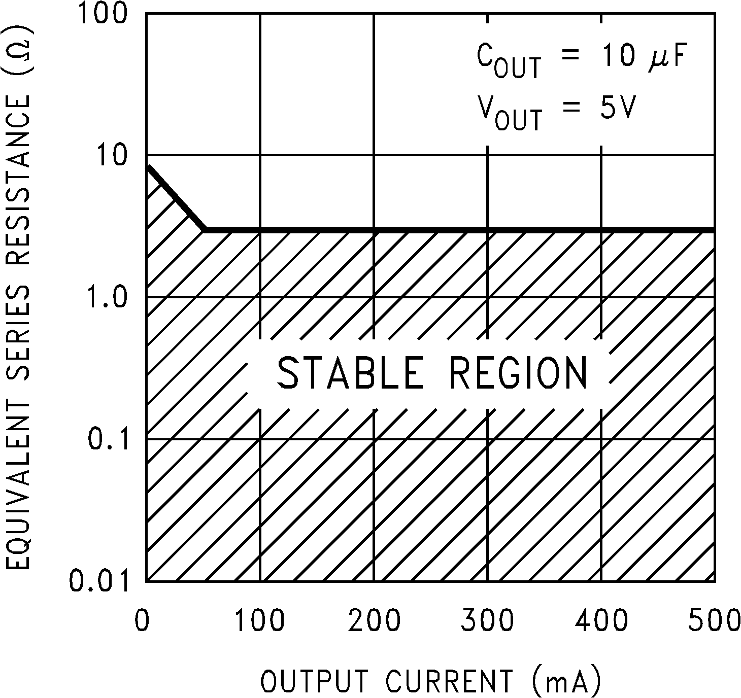 Figure 19. ESR Limits
It is important to note that for most capacitors, ESR is specified only at room temperature. However, the designer must ensure that the ESR will stay inside the limits shown over the entire operating temperature range for the design.
For aluminum electrolytic capacitors, ESR will increase by about 30X as the temperature is reduced from 25°C to −40°C. This type of capacitor is not well-suited for low temperature operation.
Solid tantalum capacitors have a more stable ESR over temperature, but are more expensive than aluminum electrolytics. A cost-effective approach sometimes used is to parallel an aluminum electrolytic with a solid Tantalum, with the total capacitance split about 75/25% with the Aluminum being the larger value.
If two capacitors are paralleled, the effective ESR is the parallel of the two individual values. The “flatter” ESR of the Tantalum will keep the effective ESR from rising as quickly at low temperatures.
8.2.2.3 Heatsinking
A heatsink may be required depending on the maximum power dissipation and maximum ambient temperature of the application. Under all possible operating conditions, the junction temperature must be within the range specified under Absolute Maximum Ratings.
To determine if a heatsink is required, the power dissipated by the regulator, PD, must be calculated.
Figure 20 below shows the voltages and currents which are present in the circuit, as well as the formula for calculating the power dissipated in the regulator:
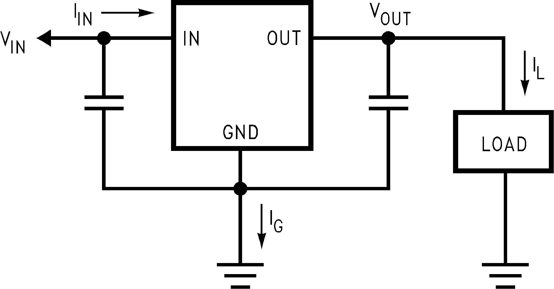
PD = (VIN − VOUT) IL + (VIN) IG
The next parameter which must be calculated is the maximum allowable temperature rise, TR (max). This is calculated by using the formula:
where
- TJ (max) is the maximum allowable junction temperature, which is 125°C for the TO-220 and TO-263 packages, and 85°C for the SOT-223 package.
- TA (max) is the maximum ambient temperature which will be encountered in the application.
Using the calculated values for TR(max) and PD, the maximum allowable value for the junction-to-ambient thermal resistance, RθJA, can now be found:
NOTE
IMPORTANT: If the maximum allowable value for RθJA is found to be ≥ 53°C/W for the TO-220 package, ≥ 80°C/W for the DDPAK/TO-263 package, or ≥ 174°C/W for the SOT-223 package, no heatsink is needed since the package alone will dissipate enough heat to satisfy these requirements.
If the calculated value for R θJA falls below these limits, a heatsink is required.
8.2.2.4 Heatsinking TO-220 Package Parts
The TO-220 can be attached to a typical heatsink, or secured to a copper plane on a PC board. If a copper plane is to be used, the values of RθJA will be the same as shown in the next section for the DDPAK/TO-263.
If a manufactured heatsink is to be selected, the value of heatsink-to-ambient thermal resistance, RθHA, must first be calculated:
where
- RθJC is defined as the thermal resistance from the junction to the surface of the case. A value of 3°C/W can be assumed for RθJC for this calculation
- RθCH is defined as the thermal resistance between the case and the surface of the heatsink. The value of RθCH will vary from about 1.5°C/W to about 2.5°C/W (depending on method of attachment, insulator, etc.). If the exact value is unknown, 2°C/W should be assumed for RθCH
When a value for RθHA is found using the equation shown, a heatsink must be selected that has a value that is less than or equal to this number.
RθHA is specified numerically by the heatsink manufacturer in the catalog, or shown in a curve that plots temperature rise vs power dissipation for the heatsink.
8.2.2.5 Heatsinking DDPAK/TO-263 and SOT-223 Package Parts
Both the DDPAK/TO-263 and SOT-223 packages use a copper plane on the PCB and the PCB itself as a heatsink. To optimize the heat sinking ability of the plane and PCB, solder the tab of the package to the plane.
Figure 21 shows for the DDPAK/TO-263 the measured values of RθJA for different copper area sizes using a typical PCB with 1 ounce copper and no solder mask over the copper area used for heatsinking.
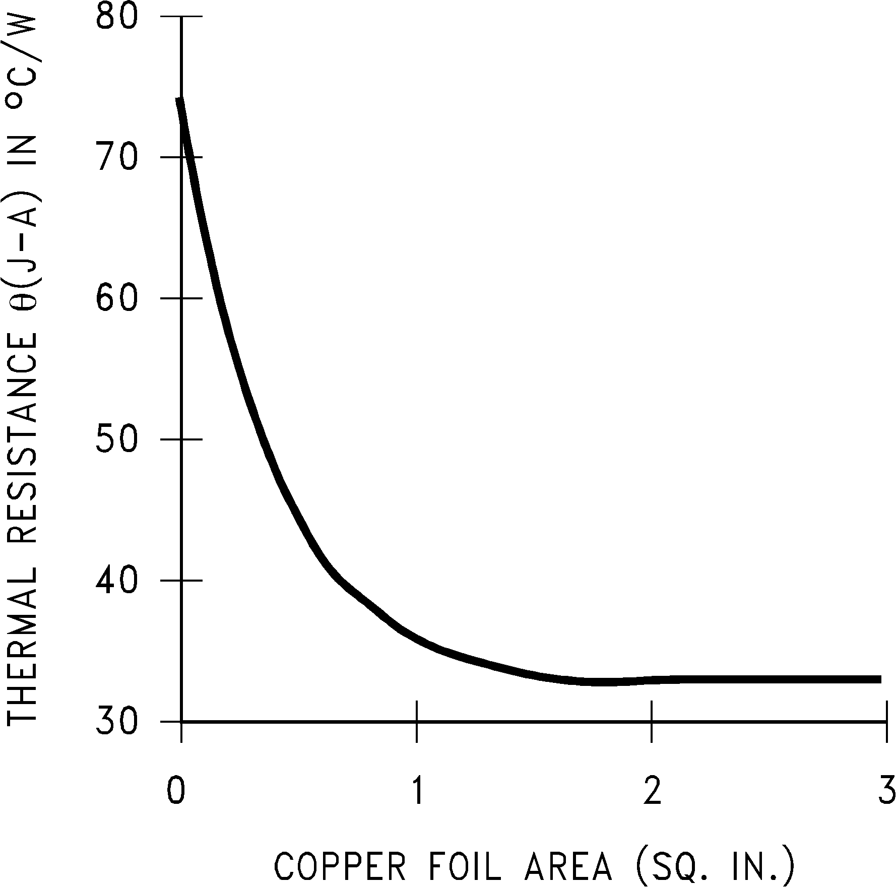 Figure 21. RθJA vs. Copper (1 ounce) Area for the DDPAK/TO-263 Package
As shown in Figure 21, increasing the copper area beyond 1 square inch produces very little improvement. It should also be observed that the minimum value of RθJA for the DDPAK/TO-263 package mounted to a PCB is 32°C/W.
As a design aid, Figure 22 shows the maximum allowable power dissipation compared to ambient temperature for the DDPAK/TO-263 device (assuming RθJA is 35°C/W and the maximum junction temperature is 125°C).
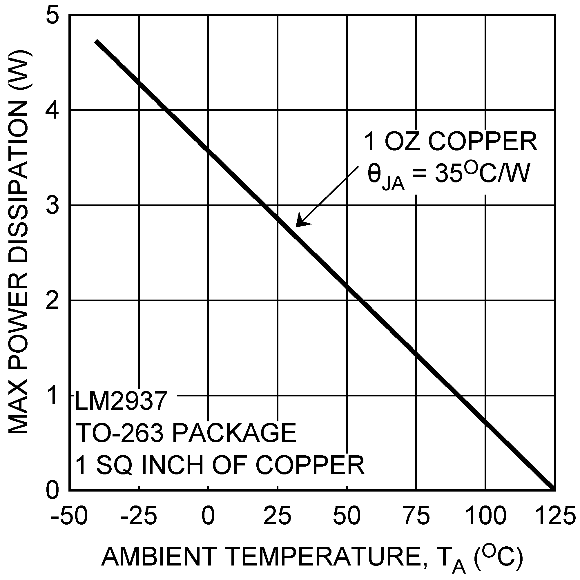 Figure 22. Maximum Power Dissipation vs. TAMB for the DDPAK/TO-263 Package
Figure 23 and Figure 24 show information for the SOT-223 package. Figure 24 assumes an RθJA of 74°C/W for 1 ounce copper and 51°C/W for 2 ounce copper and a maximum junction temperature of 85°C.
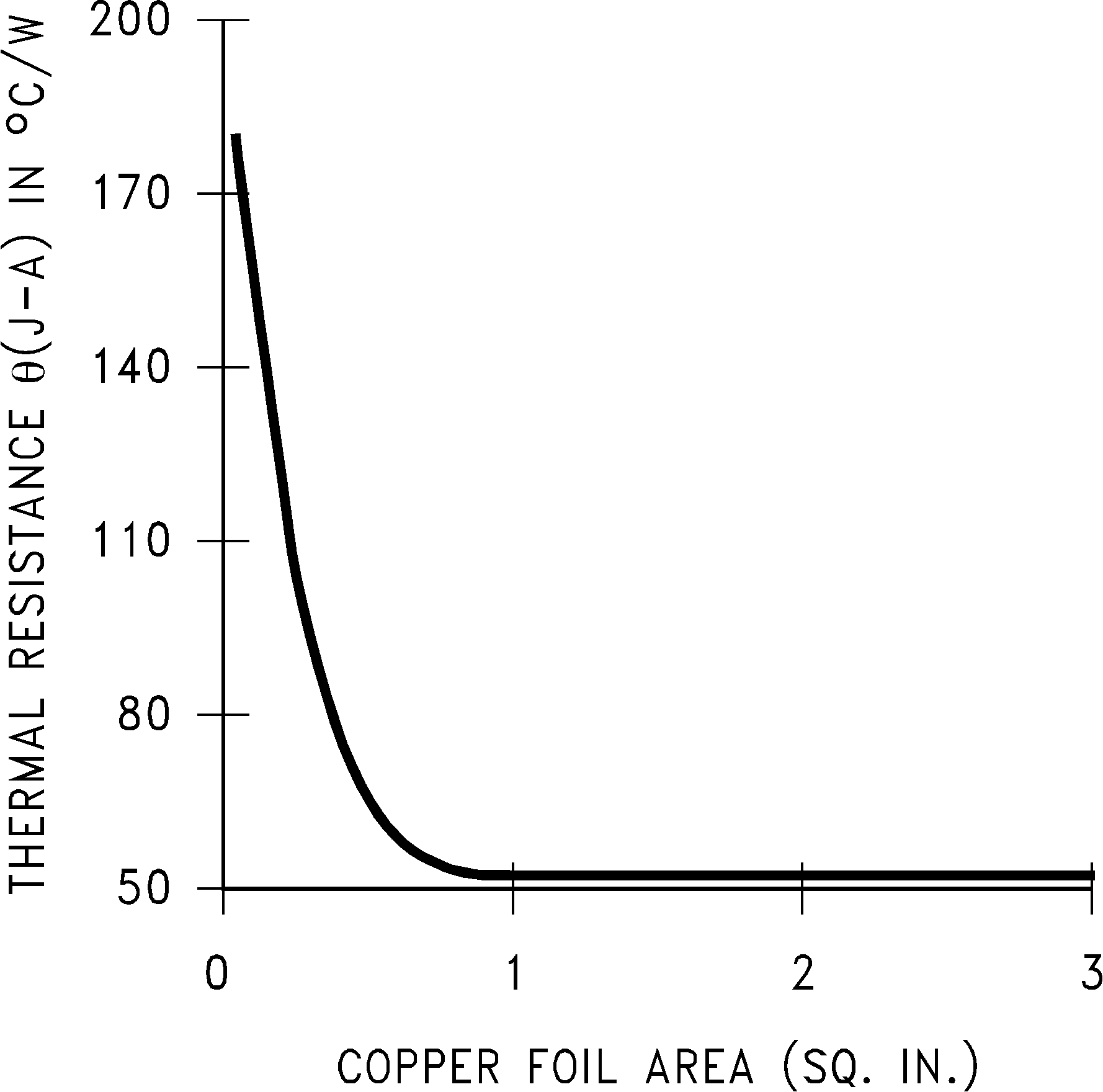 Figure 23. RθJA vs Copper (2 ounce) Area for the SOT-223 Package
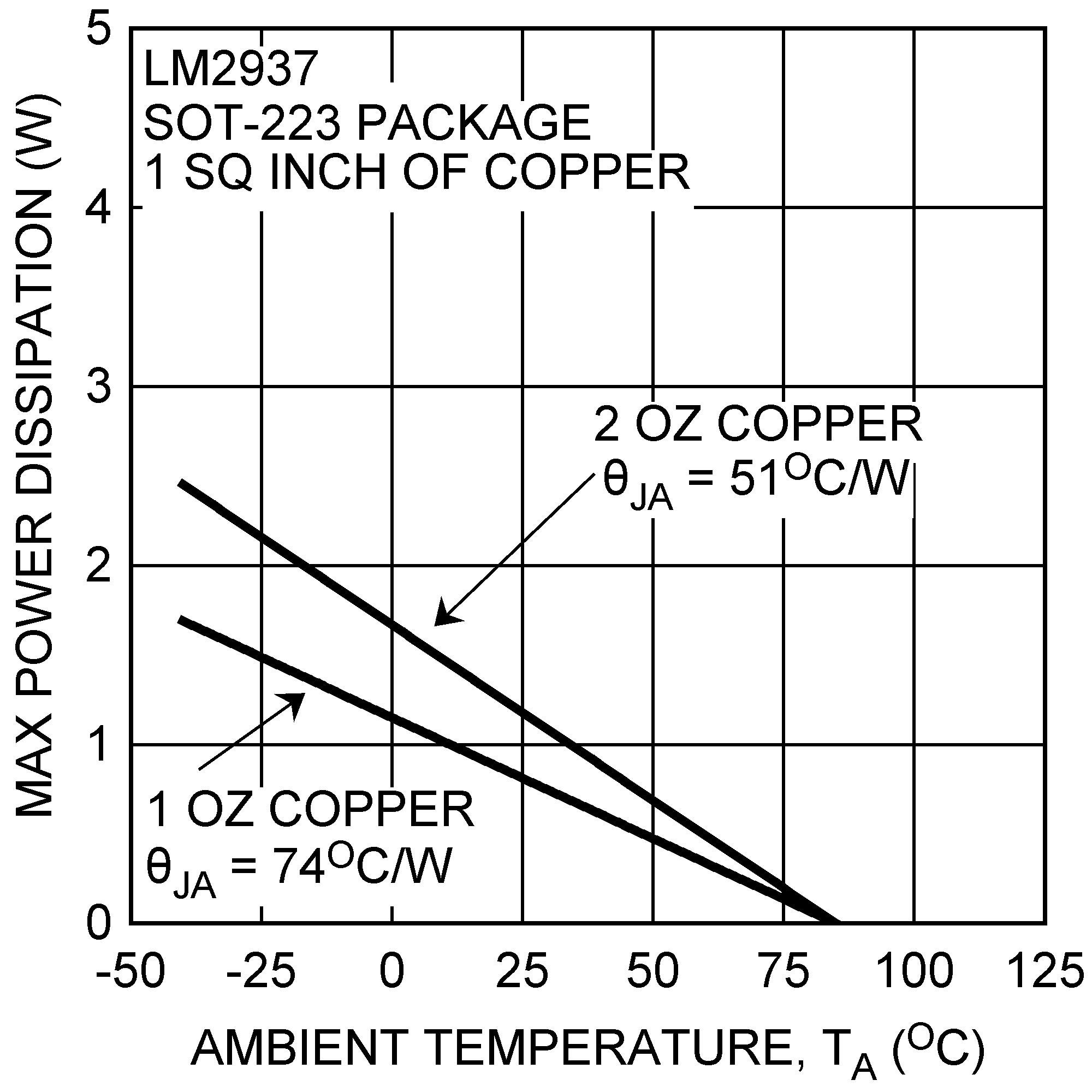 Figure 24. Maximum Power Dissipation vs TAMB for the SOT-223 Package
8.2.2.6 SOT-223 Soldering Recommendations
It is not recommended to use hand soldering or wave soldering to attach the small SOT-223 package to a printed circuit board. The excessive temperatures involved may cause package cracking.
Either vapor phase or infrared reflow techniques are preferred soldering attachment methods for the SOT-223 package.
8.2.3 Application Curves
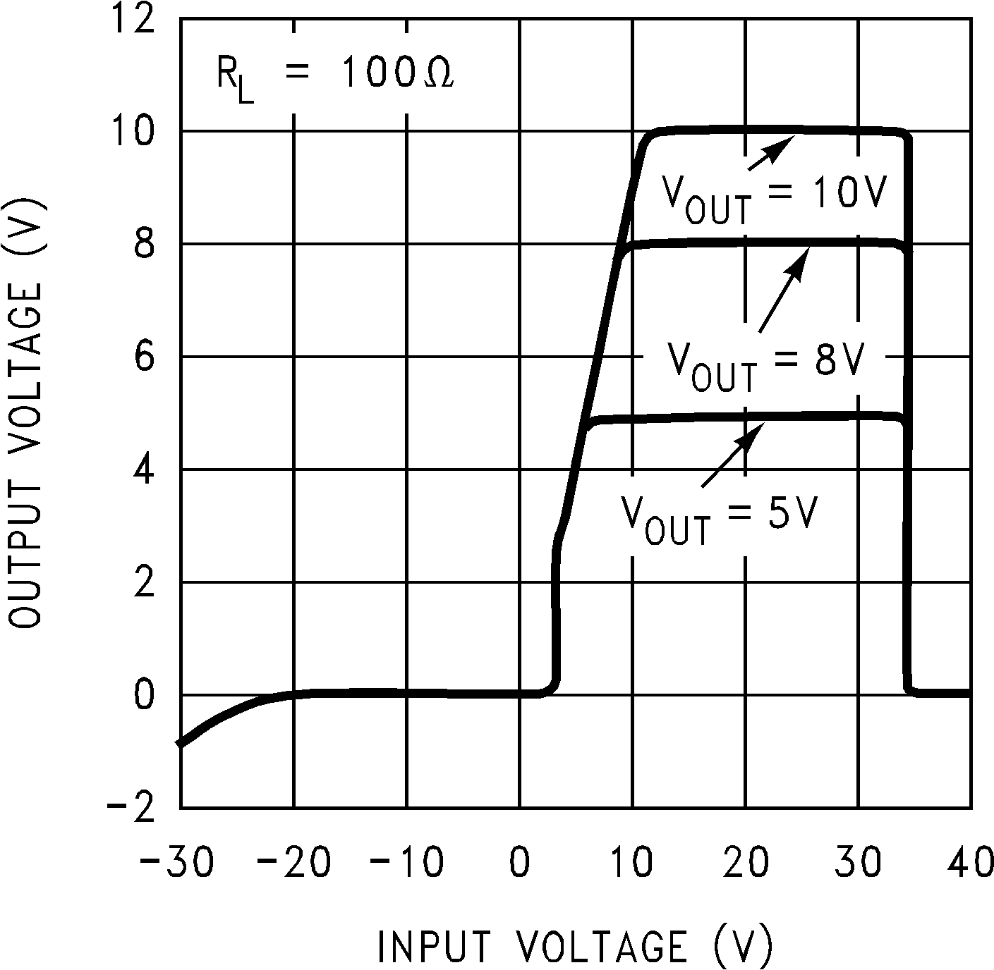 Figure 25. Output at Voltage Extremes
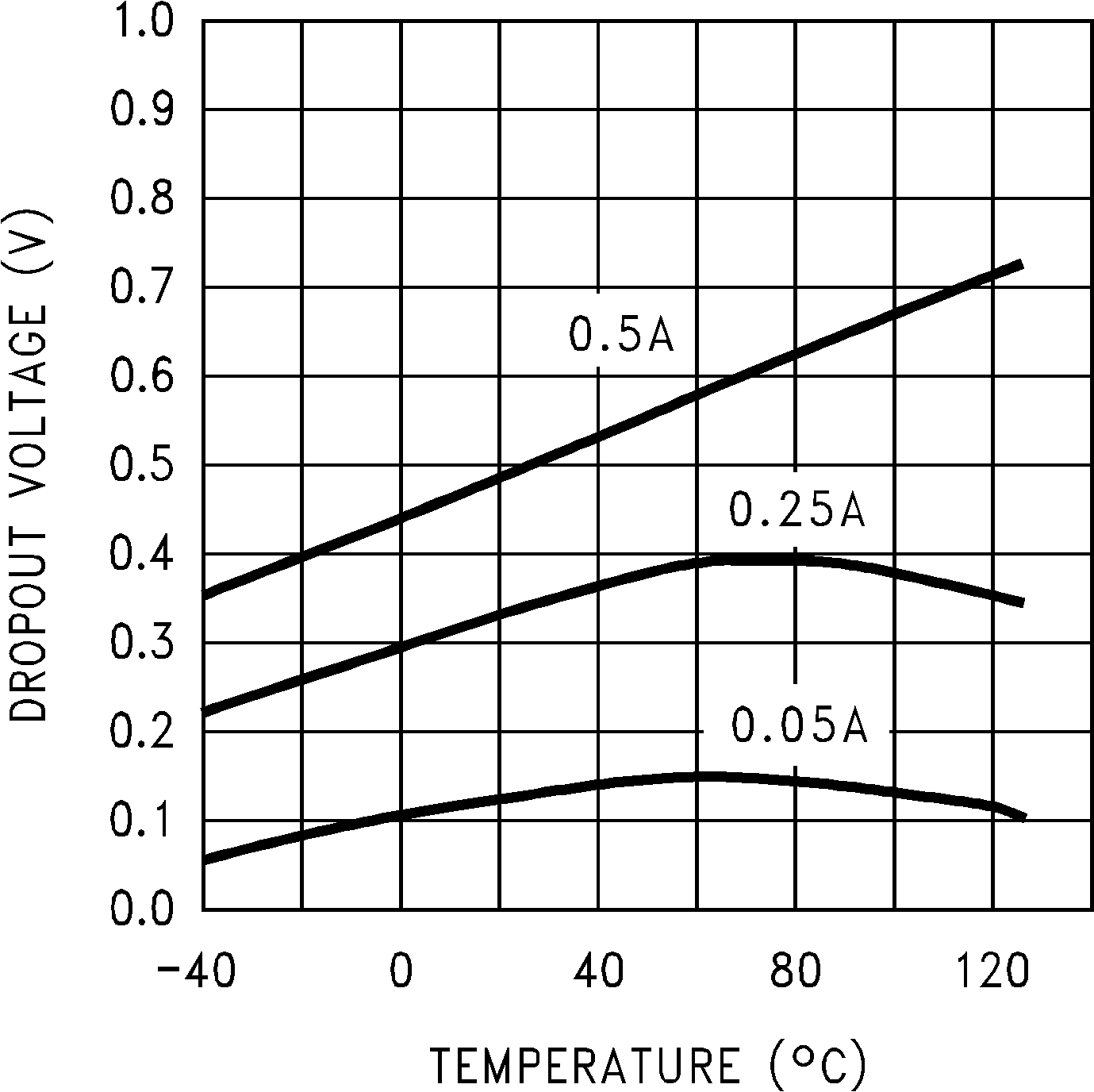 Figure 26. Dropout Voltage vs. Temperature