SNVS100F March 2000 – July 2014 LM2937
PRODUCTION DATA.
- 1 Features
- 2 Applications
- 3 Description
- 4 Revision History
- 5 Pin Configuration and Functions
-
6 Specifications
- 6.1 Absolute Maximum Ratings
- 6.2 Handling Ratings
- 6.3 Recommended Operating Conditions
- 6.4 Thermal Information
- 6.5 Electrical Characteristics: LM2937-5
- 6.6 Electrical Characteristics: LM2937-8
- 6.7 Electrical Characteristics: LM2937-10
- 6.8 Electrical Characteristics: LM2937-12
- 6.9 Electrical Characteristics: LM2937-15
- 6.10 Typical Characteristics
- 7 Detailed Description
- 8 Application and Implementation
- 9 Power Supply Recommendations
- 10Layout
- 11Device and Documentation Support
- 12Mechanical, Packaging, and Orderable Information
Package Options
Mechanical Data (Package|Pins)
Thermal pad, mechanical data (Package|Pins)
Orderable Information
5 Pin Configuration and Functions
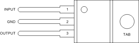
TO-220 Plastic Package (NDE)
3
Top View
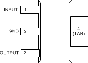
SOT-223 Plastic Package (DCY)
4
Top View
DDPAK/TO-263 Surface-Mount Package (KTT)
3
Top View
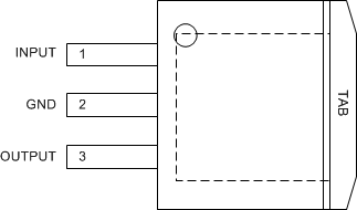
Pin Functions
| PIN | I/O | DESCRIPTION | |||
|---|---|---|---|---|---|
| NAME | NDE | KTT | DCY | ||
| INPUT | 1 | 1 | 1 | I | Unregulated voltage input |
| GND | 2 | 2 | 2 | — | Ground |
| OUTPUT | 3 | 3 | 3 | O | Regulated voltage output. This pin requires an output capacitor to maintain stability. See the Detailed Design Procedure section for output capacitor details. |
| GND | TAB | TAB | 4 | — | Thermal and ground connection. Connect the TAB to a large copper area to remove heat from the device. The TAB is internally connected to device pin 2 (GND). Connect the TAB to GND or leave floating. Do not connect the TAB to any potential other than GND at device pin 2. |