SNVS421H January 2006 – October 2017 LM3100
PRODUCTION DATA.
- 1 Features
- 2 Applications
- 3 Description
- 4 Revision History
- 5 Pin Configuration and Functions
- 6 Specifications
- 7 Detailed Description
- 8 Applications and Implementation
- 9 Layout
- 10Device and Documentation Support
- 11Mechanical, Packaging, and Orderable Information
Package Options
Mechanical Data (Package|Pins)
- PWP|20
Thermal pad, mechanical data (Package|Pins)
- PWP|20
Orderable Information
7 Detailed Description
7.1 Overview
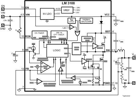
The LM3100 Step Down Switching Regulator features all functions needed to implement a cost effective, efficient buck power converter capable of supplying 1.5 A to a load. This voltage regulator contains Dual 40-V N-Channel buck synchronous switches and is available in a thermally enhanced HTSSOP-20 package. The Constant ON-Time (COT) regulation scheme requires no loop compensation, results in fast load transient response, and simplifies circuit implementation. It will work correctly even with an all ceramic output capacitor network and does not rely on the output capacitor’s ESR for stability. The operating frequency remains constant with line and load variations due to the inverse relationship between the input voltage and the on-time. The valley current limit detection circuit, internally set at 1.9 A, inhibits the high-side switch until the inductor current level subsides. Please refer to the functional block diagram with a typical application circuit.
The LM3100 can be applied in numerous applications and can operate efficiently from inputs as high as 36 V. Protection features include: Thermal shutdown, VCC under-voltage lockout, gate drive under-voltage lockout.
7.2 Functional Block Diagram

7.3 Feature Description
7.3.1 Hysteretic Control Circuit Overview
The LM3100 buck DC-DC regulator employs a control scheme in which the high-side switch on-time varies inversely with the line voltage (VIN). Control is based on a comparator and the one-shot on-timer, with the output voltage feedback (FB) compared with an internal reference of 0.8 V. If the FB level is below the reference the buck switch is turned on for a fixed time determined by the input voltage and a programming resistor (RON). Following the on-time, the switch remains off for a minimum of 260 ns. If FB is below the reference at that time the switch turns on again for another on-time period. The switching will continue until regulation is achieved.
The regulator will operate in discontinuous conduction mode at light load currents, and continuous conduction mode with heavy load current. In discontinuous conduction mode (DCM), current through the output inductor starts at zero and ramps up to a peak during the on-time, then ramps back to zero before the end of the off-time. The next on-time period starts when the voltage at FB falls below the internal reference. Until then the inductor current remains zero and the load is supplied entirely by the output capacitor. In this mode the operating frequency is lower than in continuous conduction mode, and varies with load current. Conversion efficiency is maintained since the switching losses are reduced with the reduction in load and switching frequency. The discontinuous operating frequency can be calculated approximately as follows:

In continuous conduction mode (CCM), current always flows through the inductor and never reaches zero during the off-time. In this mode, the operating frequency remains relatively constant with load and line variations. The CCM operating frequency can be calculated approximately as follows:

The output voltage is set by two external resistors (RFB1, RFB2). The regulated output voltage is calculated as follows:
7.4 Device Functional Modes
7.4.1 Start-up Regulator (VCC)
The start-up regulator is integrated within LM3100. The input pin (VIN) can be connected directly to line voltage up to 36 V, with transient capability of 40 V. The VCC output regulates at 6 V, and is current limited to 65 mA. Upon power up, the regulator sources current into the external capacitor at VCC (CVCC). CVCC must be at least 680 nF for stability. When the voltage on the VCC pin reaches the under-voltage lockout threshold of 3.75 V, the buck switch is enabled and the Soft-start pin is released to allow the soft-start capacitor (CSS) to charge.
The minimum input voltage is determined by the dropout voltage of VCC regulator, and the VCC UVLO falling threshold (≊3.7 V). If VIN is less than ≊4.0 V, the VCC UVLO activates to shut off the output.
7.4.2 Regulation Comparator
The feedback voltage at FB pin is compared to the internal reference voltage of 0.8 V. In normal operation (the output voltage is regulated), an on-time period is initiated when the voltage at FB falls below 0.8 V. The buck switch stays on for the on-time, causing the FB voltage to rise above 0.8 V. After the on-time period, the buck switch stays off until the FB voltage falls below 0.8 V again. Bias current at the FB pin is nominally 100 nA.
7.4.3 Over-Voltage Comparator
The voltage at FB pin is compared to an internal 0.92 V reference. If the feedback voltage rises above 0.92 V the on-time pulse is immediately terminated. This condition can occur if the input voltage, or the output load, changes suddenly. Once the OVP is activated, the buck switch remains off until the voltage at FB pin falls below 0.92 V. The low side switch will stay on to discharge the inductor energy until the inductor current decays to zero. The low side switch will be turned off.
7.4.4 ON-Time Timer, Shutdown
The ON-Time of LM3100 main switch is determined by the RON resistor and the input voltage (VIN), and is calculated from:

The inverse relationship of tON and VIN results in a nearly constant switching frequency as VIN is varied. RON should be selected for a minimum on-time (at maximum VIN) greater than 200 ns for proper current limit operation. This requirement limits the maximum frequency for each application, depending on VIN and VOUT, calculated from Equation 5:

The LM3100 can be remotely shut down by taking the EN pin below 1.1 V. Refer to Figure 19. In this mode the SS pin is internally grounded, the on-timer is disabled, and bias currents are reduced. Releasing the EN pin allows normal operation to resume.
For normal operation, the voltage at the EN pin is set between 1.5 V and 3.0 V, depending on VIN and the external pull-up resistor. For all cases, this voltage must be limited not to exceed 7 V.
 Figure 19. Shutdown Implementation
7.4.5 Current Limit
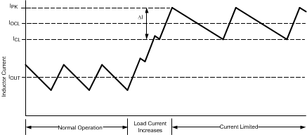
Current limit detection occurs during the off-time by monitoring the re-circulating current through the low-side synchronous switch. Referring to Functional Block Diagram, when the buck switch is turned off, inductor current flows through the load, into PGND, and through the internal low-side synchronous switch. If that current exceeds 1.9 A the current limit comparator toggles, forcing a delay to the start of the next on-time period. The next cycle starts when the re-circulating current falls back below 1.9 A and the voltage at FB is below 0.8 V. The inductor current is monitored during the low-side switch on-time. As long as the overload condition persists and the inductor current exceeds 1.9 A, the high-side switch will remain inhibited. The operating frequency is lower during an over-current due to longer than normal off-times.
Figure 20 illustrates an inductor current waveform, the average inductor current is equal to the output current, IOUT in steady state. When an overload occurs, the inductor current will increase until it exceeds the current limit threshold, 1.9 A. Then the control keeps the high-side switch off until the inductor current ramps down below 1.9 A. Within each on-time period, the current ramps up an amount equal to:

During this time the LM3100 is in a constant current mode, with an average load current (IOCL) equal to 1.9 A +ΔI/2.
 Figure 20. Inductor Current - Current Limit Operation
7.4.6 N-Channel Buck Switch and Driver
The LM3100 integrates an N-Channel buck (high-side) switch and associated floating high voltage gate driver. The gate drive circuit works in conjunction with an external bootstrap capacitor and an internal high voltage diode. A 33 nF capacitor (CBST) connected between BST and SW pins provides voltage to the high-side driver during the buck switch on-time. During each off-time, the SW pin falls to approximately –1 V and CBST charges from the VCC supply through the internal diode. The minimum off-time of 260 ns ensures adequate time each cycle to recharge the bootstrap capacitor.
7.4.7 Soft-Start
The soft-start feature allows the converter to gradually reach a steady state operating point, thereby reducing start-up stresses and current surges. Upon turn-on, after VCC reaches the under-voltage threshold, an internal 8 µA current source charges up the external capacitor at the SS pin. The ramping voltage at SS (and the non-inverting input of the regulation comparator) ramps up the output voltage in a controlled manner.
An internal switch grounds the SS pin if any of the following cases happen: (i) VCC falls below the under-voltage lock-out threshold; (ii) a thermal shutdown occurs; or (iii) the EN pin is grounded. Alternatively, the converter can be disabled by connecting the SS pin to ground using an external switch. Releasing the switch allows the SS pin return to pull high and the output voltage returns to normal. The shut-down configuration is shown in Figure 21 .
 Figure 21. Alternate Shutdown Implementation
7.4.8 Thermal Protection
The LM3100 should be operated so the junction temperature does not exceed the maximum limit. An internal Thermal Shutdown circuit, which activates (typically) at 165°C, takes the controller to a low power reset state by disabling the buck switch and the on-timer, and grounding the SS pin. This feature helps prevent catastrophic failures from accidental device overheating. When the junction temperature falls back below 145°C (typical hysteresis = 20°C), the SS pin is released and normal operation resumes.