SNVS970C March 2013 – October 2014 LM3279
PRODUCTION DATA.
- 1 Features
- 2 Applications
- 3 Description
- 4 Revision History
- 5 Pin Configuration and Functions
- 6 Specifications
- 7 Detailed Description
- 8 Application and Implementation
- 9 Power Supply Recommendations
- 10Layout
- 11Device and Documentation Support
- 12Mechanical, Packaging, and Orderable Information
Package Options
Mechanical Data (Package|Pins)
- YZR|16
Thermal pad, mechanical data (Package|Pins)
Orderable Information
8 Application and Implementation
NOTE
Information in the following applications sections is not part of the TI component specification, and TI does not warrant its accuracy or completeness. TI’s customers are responsible for determining suitability of components for their purposes. Customers should validate and test their design implementation to confirm system functionality.
8.1 Application Information
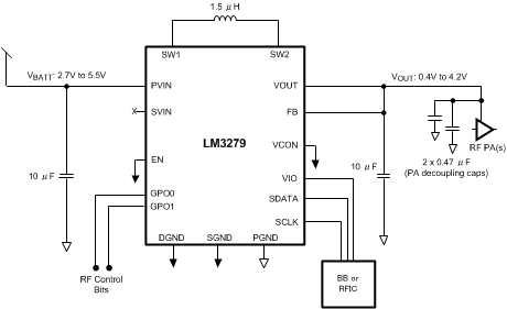
The LM3279 is a high-efficiency buck boost DC-DC converter optimized to power 3G/4G power amplifier in cell phones, portable communication devices, or other battery-powered RF devices. The device is designed to operate from an input supply voltage between 2.7 V and 5.5 V with a maximum load current of 1 A. It operates in PWM mode for medium-to-heavy load conditions and in PFM mode for light load conditions to optimize for best efficiency, transient performance, and output voltage ripple at varying load conditions. In PWM mode the LM3279 converter operates with nominal switching frequency of 2.4 MHz, thus enabling use of smaller size capacitors and inductor. The converter operates in PFM mode at lighter load conditions to maintain high efficiency. The LM3279 switches between PFM and PWM based on load current and /or the output voltage, and Figure 24 shows one of many application configurations for LM3279. A battery-connected system provides input supply to LM3279 which in turn very efficiently converts this input to a variable output with superior transient response and output noise, thereby saving the 3G/4G power amplifiers from having to operate from a higher supply voltage, such as a direct connection to a battery. This results in significant power dissipation savings and consequently cooler operation and also lower current consumption for the power amplifier without sacrificing its RF performance. In applications where low voltage battery operation is a significant feature; the buck-boost can seamlessly transition to boost and power the 3G/4G PA for high peak-to-average ratio signals as well.
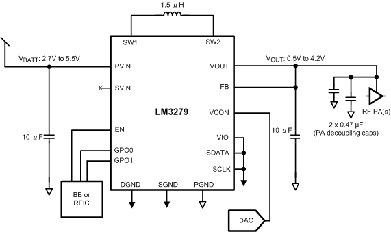
To control the output voltage there are two methods in which the LM3279 can be used : Analog Control where an analog control voltage (VCON) which is equal to VOUT/3 need to feed into the LM3279 from an external DAC. In the digital mode RFFE signaling is used to control the register address 0x00 to set the output voltage, and the LM3279 acts as a slave device on the RFFE bus.
8.2 Typical Application
8.2.1 Typical Application Circuit: Digital Control
 Figure 24. LM3279 Digital Control
8.2.1.1 Design Requirements
The LM3279 buck-boost converter has internal loop compensation. Therefore, the external LC filter has to be selected according to the internal compensation. Nevertheless, it's important to consider, that the effective inductance, due to inductor tolerance and current derating can vary between 20% and –30%. The same for the capacitance of the output filter: the effective capacitance can vary between 20% and –50% of the specified datasheet value, due to capacitor tolerance and bias voltage. For this reason Table 3 and Table 4 show the typical inductor and capacitor used with the LM3279 device.
8.2.1.2 Detailed Design Procedure
8.2.1.2.1 Output Current Capability
The typical LM3279 load capability vs. input voltage is as shown in Table 2. There are 3 distinct regions of current capability. In the low output-voltage region, VOUT < 2.1 V (also known as the RDSON-managed region), the output-current capability is determined by the current capability of the RDSON-managed MOSFET, typically 600 mA. When the output voltage is greater than 2.1 V, and in buck mode, the current capability increases to 1400 mA as determined by the overcurrent limit setting and the magnitude of ripple current. While in boost-mode operation, the output-current capability is determined by the output-input voltage ratio. It is expected for the typical RF PA to have an approximate resistive load characteristic. Refer to Table 2 for output current capability.
Table 2. Output Voltage vs Maximum Output Current Derating
| VOUT (V) | VIN (V) | MAXIMUM IOUT CAPABILITY (mA) |
|---|---|---|
| 4.2 | ≤ 3 | 450 |
| > 3 | 650 | |
| 3.8 | ≥ 2.5 | 500 |
| ≥ 2.7 | 750 | |
| ≥ 3 | 950 | |
| 3.4 | ≥ 2.5 | 750 |
| ≥ 2.7 | 950 | |
| ≥ 3 | 1100 | |
| < 1.5 | 2.7 to 5 | 100 (in PFM mode) |
8.2.1.2.2 Recommended External Components
8.2.1.2.2.1 Inductor Selection
A 1.5-µH inductor with a saturation current rating over 1900 mA and low inductance drop at the full DC bias condition is recommended for almost all applications. An inductor with a DC resistance of less than 0.1 Ω and smaller ESR should be used to get good efficiency for all output current conditions.
Table 3. Suggested Inductors
| MODEL | VENDOR | DIMENSIONS (mm) | ISAT mA (30% DROP IN INDUCTANCE) |
DCR (mΩ) |
|---|---|---|---|---|
| DFE201610C-1R5M (1285A5-H-1R5M) (1.5 µH) |
TOKO | 2.0 x 1.6 x 1.0 | 2200 | 120 |
| TFM201610A-1R5M (1.5 µH) | TDK | 2.0 x 1.6 x 1.0 | 2000 | 140 |
| ELGUEA1R5NA (1.5 μH) | Panasonic | 2.0 x 1.6 x 1.0 | 1900 | 100 |
If a smaller inductance inductor is used in the application, the VOUT transient response time is affected. If a winding type inductor is used, the efficiency at light load current condition may not be so good due to bigger DCR.
8.2.1.2.2.2 Input Capacitor Selection
A ceramic input capacitor of 10 µF, 6.3V, 0402 or higher is sufficient for most applications. Place the input capacitor as close as possible to the PVIN pin and PGND pin of the device. A larger value of higher voltage rating may be used to improve input filtering. Use X7R, X5R, or B types; do not use Y5V or F. The input filter capacitor supplies current to the PFET (high-side) switch in the first half of each cycle and reduces voltage ripple imposed on the input power source. A ceramic capacitor’s low ESR provides the best noise filtering of the input voltage spikes due to this rapidly changing current.
8.2.1.2.3 Output Capacitor Selection
Use a 10-µF, 6.3-V, 0402 capacitor for the output capacitor. Use of capacitor types such as X5R, X7R is recommended for the filter. These provide an optimal balance between small size, cost, reliability, and performance for cell phones and similar applications. Table 4 lists suggested part numbers and suppliers. DC bias characteristics of the capacitors must be considered while selecting the voltage rating and case size of the capacitor. Smaller case sizes for the output capacitor mitigate piezo-electric vibrations of the capacitor when the output voltage is stepped up and down at fast rates. However, they have a bigger percentage drop in value with DC bias. A 0402 case size output capacitor is recommended for small solution size. For RF Power Amplifier applications, the output capacitor loading is combined between the DC-DC converter and the RF Power Amplifier(s). (10 μF (0402) + PA input cap 3 x 1μF (0402/0201) is recommended.) The optimum capacitance split is application-dependent. Place all the output capacitors very close to their respective device. If using a 4.7 μF, 0402 as the output capacitor, the total recommended actual capacitance on the VOUT bus should be at least > 6.8 μF (4.7 μF + PA decoupling caps), to take into account the 0402 DC bias degradation and other tolerances. The minimum capacitance under DC bias conditions should be > 3 μF.
Table 4. Suggested Capacitors
| MODEL | VENDOR |
|---|---|
| 10 µF for CIN = COUT | |
| CL05A106MQ5NUN (0402) | Samsung |
| 1.0 µF for PA Decoupling Caps (x 3) | |
| C0603X5R0G105M(0201(0603)) | TDK |
| 0.47 µF for PA Decoupling Caps (x 2) | |
| GRM033R60J474ME90 (0201(0603)) | Murata |
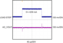
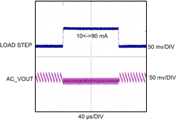
8.2.1.3 Application Curves

| VOUT = 3.5 V | PVIN = 3.8 V | |

| VOUT = 0.8 V | PVIN = 4.2 V | |
8.2.2 Typical Application Circuit: Analog Control
 Figure 27. LM3279 Analog Control
8.2.2.1 Design Requirements
See Design Requirements above.
8.2.2.2 Detailed Design Procedure
See Detailed Design Procedure above.
8.2.2.3 Application Curves
See Application Curves above.