SNVS450F September 2006 – October 2015 LM3402 , LM3402HV
PRODUCTION DATA.
- 1 Features
- 2 Applications
- 3 Description
- 4 Revision History
- 5 Pin Configuration and Functions
- 6 Specifications
- 7 Detailed Description
-
8 Application and Implementation
- 8.1 Application Information
- 8.2 Typical Application
- 9 Power Supply Recommendations
- 10Layout
- 11Device and Documentation Support
- 12Mechanical, Packaging, and Orderable Information
Package Options
Mechanical Data (Package|Pins)
Thermal pad, mechanical data (Package|Pins)
Orderable Information
10 Layout
10.1 Layout Guidelines
The performance of any switching converter depends as much upon the layout of the PCB as the component selection. The following guidelines will help the user design a circuit with maximum rejection of outside EMI and minimum generation of unwanted EMI.
10.1.1 Compact Layout
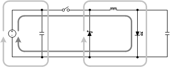
Parasitic inductance can be reduced by keeping the power path components close together and keeping the area of the loops that high currents travel small. Short, thick traces or copper pours (shapes) are best. In particular, the switch node (where L1, D1, and the SW pin connect) should be just large enough to connect all three components without excessive heating from the current it carries. The LM3402/HV operates in two distinct cycles whose high current paths are shown in Figure 22:
 Figure 31. Buck Converter Current Loops
The dark grey, inner loop represents the high current path during the MOSFET ON-time. The light grey, outer loop represents the high current path during the off-time.
10.1.2 Ground Plane and Shape Routing
The diagram of Figure 22 is also useful for analyzing the flow of continuous current vs the flow of pulsating currents. The circuit paths with current flow during both the ON-time and off-time are considered to be continuous current, while those that carry current during the ON-time or off-time only are pulsating currents. Preference in routing should be given to the pulsating current paths, as these are the portions of the circuit most likely to emit EMI. The ground plane of a PCB is a conductor and return path, and it is susceptible to noise injection just as any other circuit path. The continuous current paths on the ground net can be routed on the system ground plane with less risk of injecting noise into other circuits. The path between the input source and the input capacitor and the path between the recirculating diode and the LEDs/current sense resistor are examples of continuous current paths. In contrast, the path between the recirculating diode and the input capacitor carries a large pulsating current. This path should be routed with a short, thick shape, preferably on the component side of the PCB. Multiple vias in parallel should be used right at the pad of the input capacitor to connect the component side shapes to the ground plane. A second pulsating current loop that is often ignored is the gate drive loop formed by the SW and BOOT pins and capacitor CB. To minimize this loop at the EMI it generates, keep CB close to the SW and BOOT pins.
10.1.3 Current Sensing
The CS pin is a high-impedance input, and the loop created by RSNS, RZ (if used), the CS pin and ground should be made as small as possible to maximize noise rejection. RSNS should therefore be placed as close as possible to the CS and GND pins of the IC.
10.1.4 Remote LED Arrays
In some applications the LED or LED array can be far away (several inches or more) from the LM3402/HV, or on a separate PCB connected by a wiring harness. When an output capacitor is used and the LED array is large or separated from the rest of the converter, the output capacitor should be placed close to the LEDs to reduce the effects of parasitic inductance on the AC impedance of the capacitor. The current sense resistor should remain on the same PCB, close to the LM3402/HV.
10.2 Layout Example
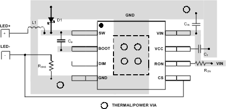
 Figure 32. Layout Recommendation