SNVS656D September 2010 – October 2016 LM3492 , LM3492-Q1
PRODUCTION DATA.
- 1 Features
- 2 Applications
- 3 Description
- 4 Revision History
- 5 Description (continued)
- 6 Pin Configuration and Functions
- 7 Specifications
-
8 Detailed Description
- 8.1 Overview
- 8.2 Functional Block Diagram
- 8.3 Feature Description
- 8.4 Device Functional Modes
- 8.5 Programming
- 9 Application and Implementation
- 10Power Supply Recommendations
- 11Layout
- 12Device and Documentation Support
- 13Mechanical, Packaging, and Orderable Information
Package Options
Mechanical Data (Package|Pins)
- PWP|20
Thermal pad, mechanical data (Package|Pins)
- PWP|20
Orderable Information
9 Application and Implementation
NOTE
Information in the following applications sections is not part of the TI component specification, and TI does not warrant its accuracy or completeness. TI’s customers are responsible for determining suitability of components for their purposes. Customers should validate and test their design implementation to confirm system functionality.
9.1 Application Information
The LM3492/-Q1 device is ideal for automotive and marine GPS display and applications that require a high contrast ratio.
9.2 Typical Application
9.2.1 Design Requirements
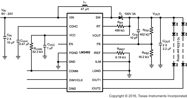
The following procedures are to design an LED driver using the LM3492/-Q1 with an input voltage ranged from 9 V to 24 V and two LED strings consists of 10 LEDs each with a forward voltage of 3.8 V for each LED when running at 200 mA. The output power is 15.2 W. The switching frequency fSW is designed to be 300 kHz.
9.2.2 Detailed Design Procedure
9.2.2.1 RFB1, RFB2, and CFB
The nominal voltage of the LED string with 10 LEDs is 38 V, and the minimum voltage of the IOUTn pin (n = 1, 2) is 1 V when ILED is 200 mA. As a result, VOUT(nom) is 39 V. Design VOUT(max) to be 65 V. From Equation 5, VFB(nom) is approximately 1.5 V, which falls in the recommended operation range from 1.05 V to 2 V. Also, design RFB2 to be 16.2 kΩ. From Equation 3, RFB1 is calculated to be 405 kΩ, and a standard resistor value of 402 kΩ is selected. CFB is selected to be 10 pF as recommended.
9.2.2.2 L1
The main parameter affected by the inductor is the peak to peak inductor current ripple (ILR). To maintain a continuous conduction mode (CCM) operation, ensure that the average inductor current IL1 is larger than half of ILR. For a boost converter, IL1 equals to the input current IIN. Hence,
Also,
If VIN is maximum, which is 24 V in this example, and only one LED string is turned on (because the two channels of the device are individually dimmable), IIN is minimum. From Equation 7 to Equation 9, it can be calculated that IIN(MIN), ton, and L1 are 0.325 A, 1.28 µs, and 47 µH. However, from Equation 7, IIN is maximum when VIN is minimum, which is 9 V in this example, and the two LED strings are turned on together. Hence IIN(max) is 1.73 A. Then, ILR is
From Equation 8, ton is 2.56 µs. From (9), ILR is 0.49 A. The steady-state peak inductor current IL1(PEAK) is
As a result, IL1(PEAK) is 1.98 A. A standard value of 47 µH is selected for L1, and its saturation current is larger than 1.98 A.
9.2.2.3 D1
The selection of the boost diode D1 depends on two factors. The first factor is the reverse voltage, which equals to VOUT for a boost converter. The second factor is the peak diode current at the steady state, which equals to the peak inductor current as shown in Equation 11. In this example, a 100-V, 3-A Schottky diode is selected.
9.2.2.4 CIN and COUT
The function of the input capacitor CIN and the output capacitor COUT is to reduce the input and output voltage ripples. Experimentation is usually necessary to determine their value. The rated DC voltage of capacitors used should be higher than the maximum DC voltage applied. Owing to the concern of product lifetime, TI recommends ceramic capacitors. But ceramic capacitors with high rated DC voltage and high capacitance are rare in general. Multiple capacitors connecting in parallel can be used for CIN and COUT. In this example, two 10-µF ceramic capacitor are used for CIN, and two 2.2-µF ceramic capacitor are used for COUT.
9.2.2.5 CVCC
The capacitor on the VCC pin provides noise filtering and stabilizes the LDO regulator. It also prevents false triggering of the VCC UVLO. CVCC is recommended to be a 1-µF, good quality and low ESR ceramic capacitor.
9.2.2.6 CCDHC
The capacitor at the CDHC pin not only affects the sensitivity of the DHC but also determines the soft-start time tSS, the time for the output voltage to rise until power good. tSS is determined from the following equation:

In this example, CCDHC is recommended to be a 0.47-µF good quality and low ESR ceramic capacitor.
9.2.2.7 RRT and RIREF
The resistors RRT and RIREF set the switching frequency fSW of the boost converter and the LED current ILED respectively. From Figure 16, if fSW is 300 kHz, RRT is selected to be 442 kΩ. From Figure 21, if ILED is 200 mA, RIREF is selected to be 6.19 kΩ.
9.2.2.8 RCOMM
Because the COMM pin is open drain, a resistor RCOMM of 52.3 kΩ is used to connect the VCC and COMM pins to act as a pullup function.
9.2.3 Application Curve
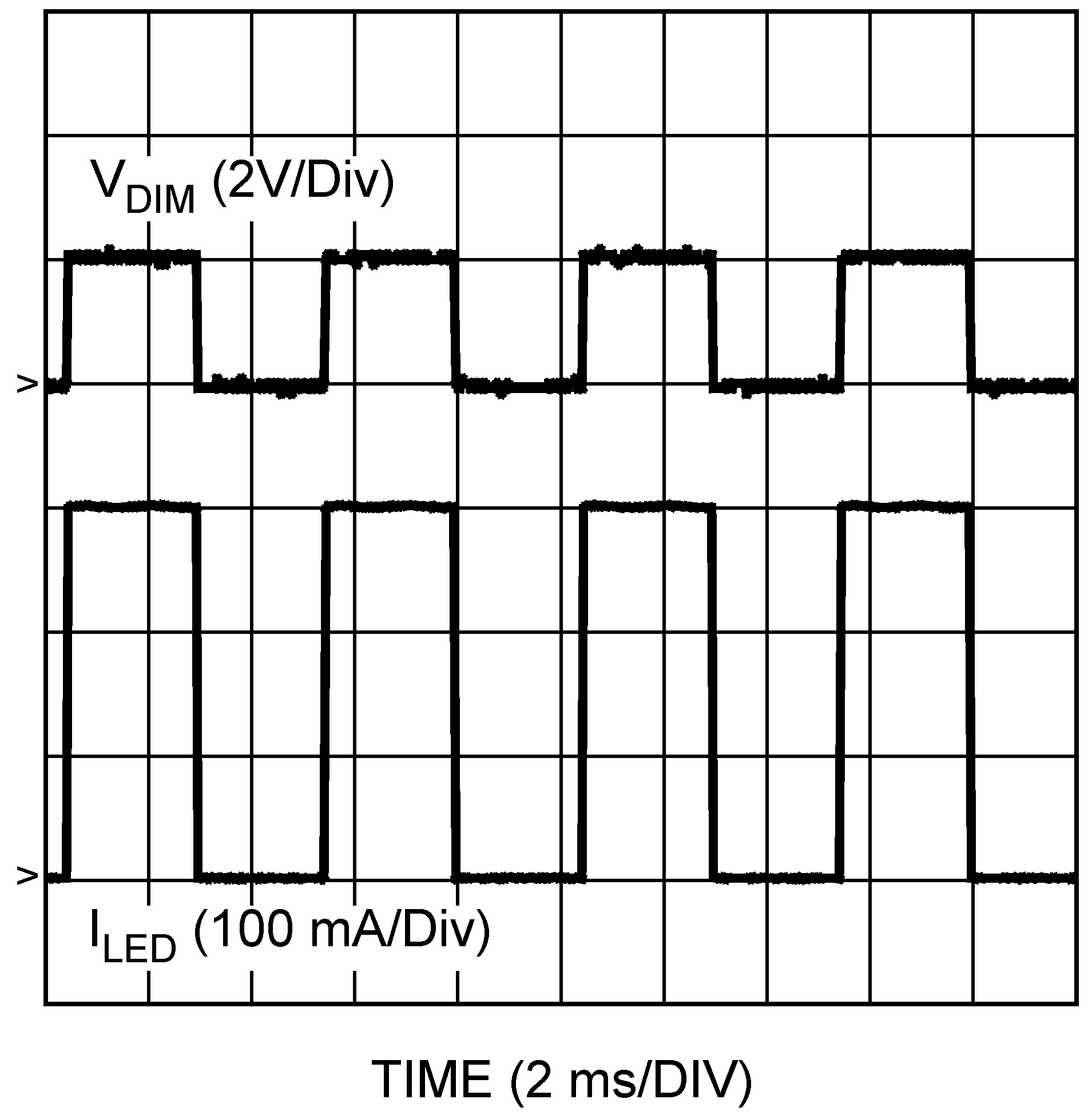
 Figure 27. LED 50% Dimming, Both Channels Combined
(VIN = 12 V, ILED = 150 mA, 200 Hz)
