SNVS606L June 2009 – December 2014 LM3530
PRODUCTION DATA.
- 1 Features
- 2 Applications
- 3 Description
- 4 Revision History
- 5 I2C Device Options
- 6 Pin Configuration and Functions
- 7 Specifications
-
8 Detailed Description
- 8.1 Overview
- 8.2 Functional Block Diagram
- 8.3
Feature Description
- 8.3.1 Start-Up
- 8.3.2 Light Load Operation
- 8.3.3 Ambient Light Sensor
- 8.3.4 ALS Operation
- 8.3.5 ALS Averaging Time
- 8.3.6 Zone Boundary Settings
- 8.3.7 Zone Boundary Trip Points and Hysteresis
- 8.3.8 Minimum Zone Boundary Settings
- 8.3.9 LED Current Control
- 8.3.10 Exponential or Linear Brightness Mapping Modes
- 8.3.11 PWM Input Polarity
- 8.3.12 I2C-Compatible Current Control Only
- 8.3.13 Simple Enable Disable With PWM Current Control
- 8.3.14 Ambient Light Current Control
- 8.3.15 Ambient Light Current Control + PWM
- 8.3.16 Interrupt Output
- 8.3.17 Overvoltage Protection
- 8.3.18 Hardware Enable
- 8.3.19 Thermal Shutdown
- 8.4 Device Functional Modes
- 8.5 Programming
- 8.6 Register Maps
- 9 Application and Implementation
- 10Power Supply Recommendations
- 11Layout
- 12Device and Documentation Support
- 13Mechanical, Packaging, and Orderable Information
Package Options
Mechanical Data (Package|Pins)
Thermal pad, mechanical data (Package|Pins)
Orderable Information
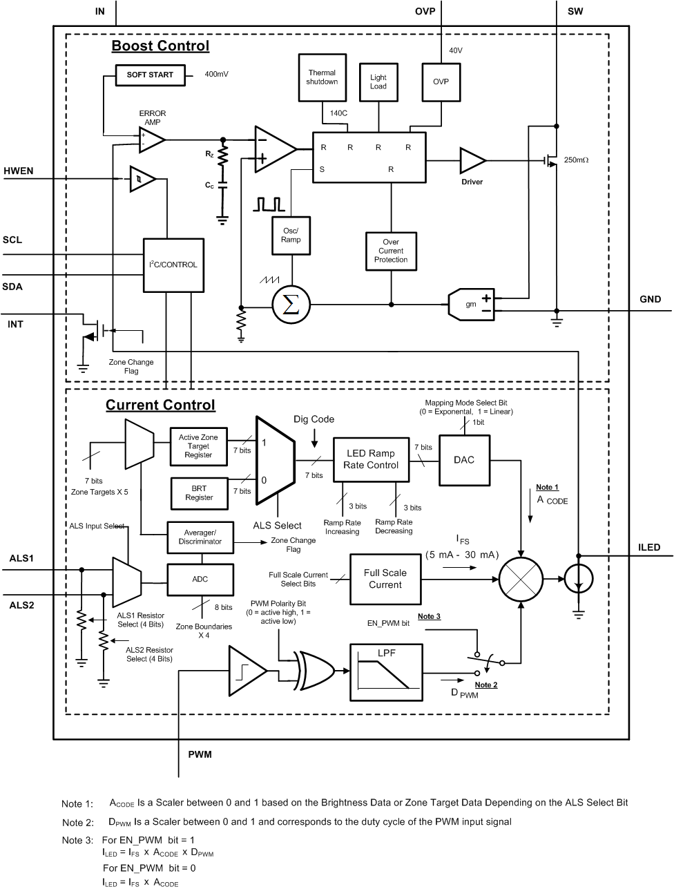
8 Detailed Description
8.1 Overview
The LM3530 utilizes an asynchronous step-up, current mode, PWM controller and regulated current sink to provide an efficient and accurate LED current for white LED bias. The device powers a single series string of LEDs with output voltages of up to 40 V and a peak inductor current of typically 839 mA. The input active voltage range is from 2.7 V to 5.5 V.
8.2 Functional Block Diagram
8.3 Feature Description
8.3.1 Start-Up
An internal soft-start prevents large inrush currents during start-up that can cause excessive current spikes at the input. For the typical application circuit (using a 10-µH inductor, a 2.2-µF input capacitor, and a 1-µF output capacitor) the average input current during start-up ramps from 0 to 300 mA in 3 ms. See Figure 22 in the Typical Characteristics.
8.3.2 Light Load Operation
The LM3530 boost converter operates in three modes: continuous conduction, discontinuous conduction, and skip mode. Under heavy loads when the inductor current does not reach zero before the end of the switching period, the device switches at a constant frequency (500 kHz typical). As the output current decreases and the inductor current reaches zero before the end of the switching period, the device operates in discontinuous conduction. At very light loads the LM3530 will enter skip mode operation causing the switching period to lengthen and the device to only switch as required to maintain regulation at the output. Light load operation provides for improved efficiency at lighter LED currents compared to continuous and discontinuous conduction. This is due to the pulsed frequency operation resulting in decreased switching losses in the boost converter.
8.3.3 Ambient Light Sensor
The LM3530 incorporates a dual input Ambient Light Sensing interface (ALS1 and ALS2) which translates an analog output ambient light sensor to a user-specified brightness level. The ambient light sensing circuit has 4 programmable boundaries (ZB0 – ZB3) which define 5 ambient brightness zones. Each ambient brightness zone corresponds to a programmable brightness threshold (Z0T – Z4T). The ALS interface is programmable to accept the ambient light information from either the highest voltage of ALS1 or ALS2, the average voltage of ALS1 or ALS2, or selectable from either ALS1 or ALS2.
Furthermore, each ambient light sensing input (ALS1 or ALS2) features 15 internal software selectable voltage setting resistors. This allows the LM3530 the capability of interfacing with a wide selection of ambient light sensors. Additionally, the ALS inputs can be configured as high impedance, thus providing for a true shutdown during low power modes. The ALS resistors are selectable through the ALS Resistor Select Register (see Table 9). Figure 26 shows a functional block diagram of the ambient light sensor input. VSNS represents the active input as described in Table 6 bits [6:5].
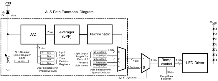 Figure 26. Ambient Light Sensor Functional Block Diagram
8.3.4 ALS Operation
The ambient light sensor input has a 0-V to 1-V operational input voltage range. LM3530 Typical Application shows the LM3530 with dual ambient light sensors (AVAGO, APDS-9005) and the internal ALS Resistor Select Register set to 0x44 (2.27 kΩ). This circuit converts 0 to 1000 LUX light into approximately a 0-mV to 850-mV linear output voltage. The voltage at the active ambient light sensor input (ALS1 or ALS2) is compared against the 8 bit values programmed into the Zone Boundary Registers (ZB0-ZB3). When the ambient light sensor output crosses one of the ZB0 – ZB3 programmed thresholds the internal ALS circuitry will smoothly transition the LED current to the new 7 bit brightness level as programmed into the appropriate Zone Target Register (Z0T – Z4T) (see Figure 27).
The ALS Configuration Register bits [6:5] programs which input is the active input, bits [4:3] control the on/off state of the ALS circuitry, and bits [2:0] control the ALS input averaging time. Additionally, the ALS Information Register is a read-only register which contains a flag (bit 3) which is set each time the active ALS input changes to a new zone. This flag is reset when the register is read back. Bits [2:0] of this register contain the current active zone information.
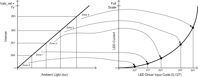 Figure 27. Ambient Light Input To Backlight Mapping
8.3.5 ALS Averaging Time
The ALS Averaging Time is the time over which the Averager block collects samples from the A/D converter and then averages them to pass to the discriminator block (see Figure 26). Ambient light sensor samples are averaged and then further processed by the discriminator block to provide rejection of noise and transient signals. The averager is configurable with 8 different averaging times to provide varying amounts of noise and transient rejection (see Table 5). The discriminator block algorithm has a maximum latency of two averaging cycles; therefore, the averaging time selection determines the amount of delay that will exist between a steady-state change in the ambient light conditions and the associated change of the backlight illumination. For example, the A/D converter samples the ALS inputs at 16 kHz. If the averaging time is set to 1024 ms then the Averager will send the updated zone information to the discriminator every 1024 ms. This zone information contains the average of 16384 samples (1024 ms × 16 kHz). Due to the latency of 2 averaging cycles, the LED current will not change until there has been a steady-state change in the ambient light for at least 2 averaging periods.
8.3.5.1 Averager Operation
The magnitude and direction (either increasing or decreasing) of the Averager output is used to determine whether the LM3530 should change brightness zones. The Averager block functions as follows:
- First, the Averager always begins with a Zone 0 reading stored at start-up. If the main display LEDs are active before the ALS block is enabled, it is recommended that the ALS Enable 1 bit is set to '1' at least 3 averaging periods before the ALS Enable 2 bit is set.
- The Averager will always round down to the lower zone in the event of a non-integer zone average. For example, if during an averaging period the ALS input transitions between zones 1 and 2 resulting in an averager output of 1.75, then the averager output will round down to 1 (see Figure 28).
- The two most current averaging samples are used to make zone change decisions.
- To make a zone change, data from three averaging cycles are needed. (Starting Value, First Transition, Second Transition or Rest).
- To Increase the brightness zone, the Averager output must have increased for at least 2 averaging periods or increased and remained at the new level for at least two averaging periods ('+' to '+' or '+' to 'Rest' in Figure 29).
- To decrease the brightness zone, the Averager output must have decreased for at least 2 averaging periods or decreased and remained at the new level for at least two averaging periods ('-' to '-' or '-' to 'Rest' in Figure 29).
In the case of two consecutive increases or decreases in the Averager output, the LM3530 will transition to zone equal to the last averager output (Figure 29).
Using the diagram for the ALS block (Figure 26), the flow of information is shown in (Figure 30). This starts with the ALS input into the A/D, into the Averager, and then into the Discriminator. Each state filters the previous output to help prevent unwanted zone to zone transitions.
When using the ALS averaging function, it is important to remember that the averaging cycle is free running and is not synchronized with changing ambient lighting conditions. Due to the nature of the averager round down, an increase in brightness can take between 2 and 3 averaging cycles to change zones, while a decrease in brightness can take between 1 and 2 averaging cycles. See Table 6 for a list of possible Averager periods. Figure 31 shows an example of how the perceived brightness change time can vary.
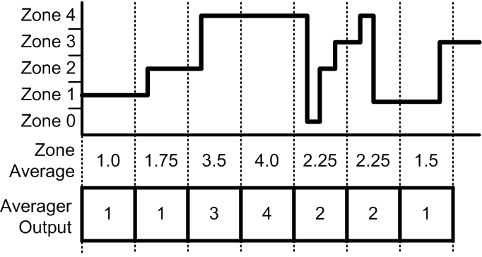 Figure 28. Averager Calculation
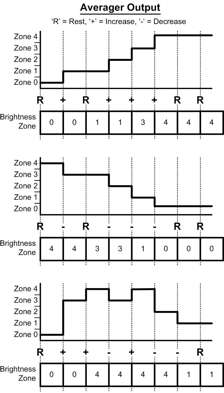 Figure 29. Brightness Zone Change Examples
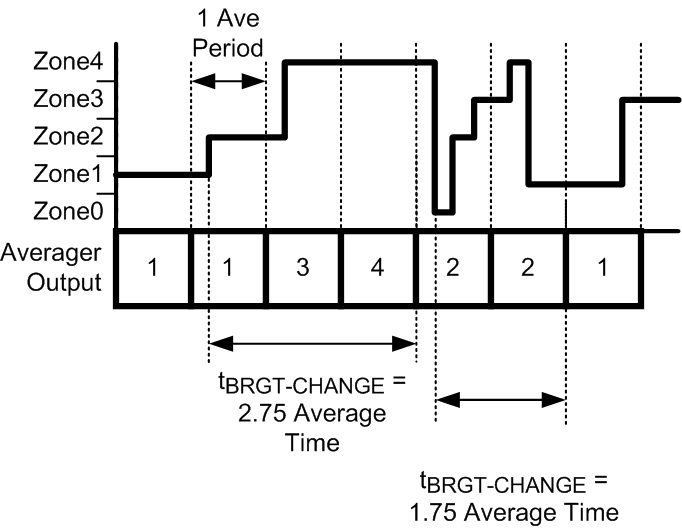 Figure 30. Ambient Light Input To Backlight Transition
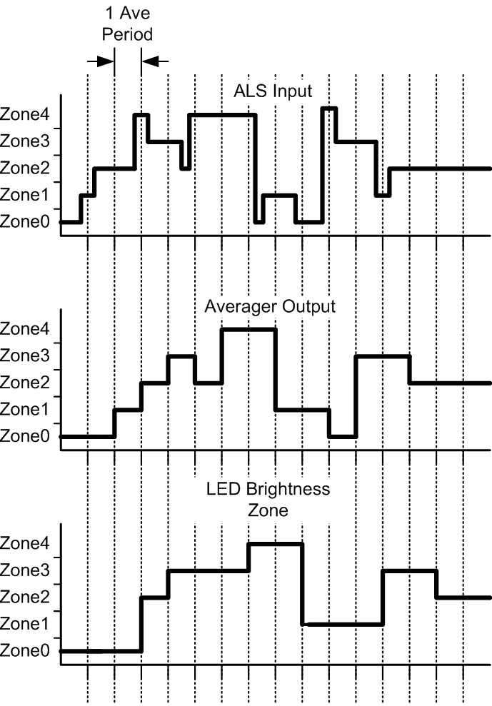 Figure 31. Perceived Brightness Change Time
8.3.6 Zone Boundary Settings
Registers 0x60, 0x61, 0x62, and 0x63 set the 4 zone boundaries (thresholds) for the ALS inputs. These 4 zone boundaries create 5 brightness zones which map over to 5 separate brightness zone targets (see Figure 27). Each 8-bit zone boundary register can set a threshold from typically 0 to 1 V with linear step sizes of approximately 1/255 = 3.92 mV. Additionally, each zone boundary has built in hysteresis which can be either lower or higher then the programmed Zone Boundary depending on the last direction (either up or down) of the ALS input voltage.
8.3.7 Zone Boundary Trip Points and Hysteresis
For each zone boundary setting, the trip point will vary above or below the nominal set point depending on the direction (either up or down) of the ALS input voltage. This is designed to keep the ALS input from oscillating back and forth between zones in the event that the ALS voltage is residing near to the programmed zone boundary threshold. The Zone Boundary Hysteresis will follow these 2 rules:
- If the last zone transition was from low to high, then the trip point (VTRIP) will be VZONE_BOUNDARY - VHYST/2, where VZONE_BOUNDARY is the zone boundary set point as programmed into the Zone Boundary registers, and VHYST is typically 7 mV.
- If the last zone transition was from high to low then the trip point (VTRIP) will be VZONE_BOUNDARY + VHYST/2.
Figure 32 details how the LM3530 ALS Input Zone Boundary Thresholds vary depending on the direction of the ALS input voltage.
Referring to Figure 32, each numbered trip point shown is determined from the direction of the previous ALS zone transition.
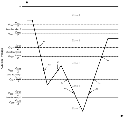 Figure 32. Zone Boundaries With Hysteresis
8.3.8 Minimum Zone Boundary Settings
The actual minimum zone boundary setting is code 0x03. Codes of 0x00, 0x01, and 0x02 are all mapped to code 0x03. Table 1 shows the Zone Boundary codes 0x00 through 0x04, the typical thresholds, and the high and low hysteresis values. The remapping of codes 0x00 - 0x02 plus the additional 4mV of offset voltage is necessary to prevent random offsets and noise on the ALS inputs from creating threshold levels that are below GND. This essentially guarantees that any Zone Boundary threshold selected is achievable with positive ALS voltages.
Table 1. Ideal Zone Boundary Settings with Hysteresis (Lower 5 Codes)
| ZONE BOUNDARY CODE | TYPICAL ZONE BOUNDARY THRESHOLD (mV) | TYPICAL THRESHOLD + HYSTERESIS (mV) | TYPICAL THRESHOLD - HYSTERESIS (mV) |
|---|---|---|---|
| 0x00 | 15.8 | 19.3 | 12.3 |
| 0x01 | 15.8 | 19.3 | 12.3 |
| 0x02 | 15.8 | 19.3 | 12.3 |
| 0x03 | 15.8 | 19.3 | 12.3 |
| 0x04 | 19.7 | 23.2 | 16.2 |
8.3.9 LED Current Control
The LED current is is a function of the Full Scale Current, the Brightness Code, and the PWM input duty cycle. The Brightness Code can either come from the BRT Register (0xA0) in I2C-Compatible Current Control, or from the ALS Zone Target Registers (Address 0x70-0x74) in Ambient Light Current Control. Figure 33 shows the current control block diagram.
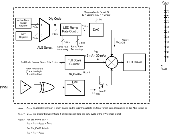 Figure 33. Current Control Block Diagram
8.3.10 Exponential or Linear Brightness Mapping Modes
With bit [1] of the General Configuration Register set to 0 (default) exponential mapping is selected and the code in the Brightness Control Register corresponds to the Full-Scale LED current percentages in Table 2 and Figure 34. With bit [1] set to 1 linear mapping is selected and the code in the Brightness Control Register corresponds to the Full-Scale LED current percentages in Table 3 and Figure 35.
8.3.11 PWM Input Polarity
Bit [6] of the General Configuration Register controls the PWM input polarity. Setting this bit to 0 (default) selects positive polarity and makes the LED current (with PWM mode enabled) a function of the positive duty cycle at PWM. With this bit set to ‘0’ the LED current (with PWM mode enabled) becomes a function of the negative duty cycle at PWM.
The PWM input is a logic level input with a frequency range of 400 Hz to 50 kHz. Internal filtering of the PWM input signal converts the duty cycle information to an average (analog) control signal which directly controls the LED current.
Example: PWM + I2C-Compatible Current Control:
As an example, assume the the General Configuration Register is loaded with (0x2D). From Table 5, this sets up the LM3530 with:
Simple Enable OFF (bit 7 = 0)
Positive PWM Polarity (bit 6 = 0)
PWM Enabled (bit 5 = 1)
Full-Scale Current set at 15.5 mA (bits [4:2] = 100)
Brightness Mapping set for Exponential (bit 1 = 0)
Device Enabled via I2C (bit 0 = 1)
Next, the Brightness Control Register is loaded with 0x73. This sets the LED current to 51.406% of full scale (see Equation 1). Finally, the PWM input is driven with a 0-V to 2-V pulse waveform at 70% duty cycle. The LED current under these conditions will be:

where
- BRT is the percentage of ILED_FS as set in the Brightness Control Register
8.3.12 I2C-Compatible Current Control Only
I2C-Compatible Control is enabled by writing a '1' to the I2C Device Enable bit (bit [0] of the General Configuration Register), a '0' to the Simple Enable bit (bit 7), and a '0' to the PWM Enable bit (bit 5). With bit 5 = 0, the duty cycle information at the PWM input is not used in setting the LED current.
In this mode the LED current is a function of the Full-Scale LED current bits (bits [4:2] of the General Configuration Register) and the code in the Brightness Control Register. The LED current mapping for the Brightness Control Register can be linear or exponential depending on bit [1] in the General Configuration Register (see Exponential or Linear Brightness Mapping Modes section). Using I2C-Compatible Control Only, the Full-Scale LED Current bits and the Brightness Control Register code provides nearly 1016 possible current levels selectable over the I2C-compatible interface.
Example: I2C-Compatible Current Control Only:
As an example, assume the General Configuration Register is loaded with 0x15. From Table 5 this sets up the LM3530 with:
Simple Enable OFF (bit 7 = 0)
Positive PWM Polarity (bit 6 = 0)
PWM Disabled (bit 5 = 0)
Full-Scale Current set at 22.5mA (bits [4:2] = 101)
Brightness Mapping set for Exponential (bit 1 = 0)
Device Enabled via I2C (bit 0 = 1)
The Brightness Control Register is then loaded with 0x72 (48.438% of full-scale current from Equation 2). The LED current with this configuration becomes:

where
- BRT is the % of ILED_FS as set in the Brightness Control Register.
Next, the brightness mapping is set to linear mapping mode (bit [1] in General Configuration Register set to 1). Using the same Full-Scale current settings and Brightness Control Register settings as before, the LED current becomes:

Which is higher now since the code in the Brightness Control Register (0x72) corresponds to 89.76% of Full-Scale LED Current due to the different mapping mode given in Figure 34.
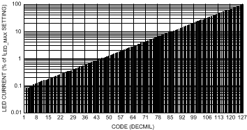 Figure 34. Exponential Brightness Mapping
Table 2. ILED vs. Brightness Register Data (Exponential Mapping)
| BRT DATA (HEX) | % FULL-SCALE CURRENT | BRT DATA (HEX) | % OF FULL-SCALE CURRENT | BRT DATA (HEX) | % OF FULL-SCALE CURRENT | BRT DATA (HEX) | % OF FULL-SCALE CURRENT |
|---|---|---|---|---|---|---|---|
| 0x00 | 0.00% | 0x20 | 0.500% | 0x40 | 2.953% | 0x60 | 17.813% |
| 0x01 | 0.080% | 0x21 | 0.523% | 0x41 | 3.125% | 0x61 | 18.750% |
| 0x02 | 0.086% | 0x22 | 0.555% | 0x42 | 3.336% | 0x62 | 19.922% |
| 0x03 | 0.094% | 0x23 | 0.586% | 0x43 | 3.500% | 0x63 | 20.859% |
| 0x04 | 0.102% | 0x24 | 0.617% | 0x44 | 3.719% | 0x64 | 22.266% |
| 0x05 | 0.109% | 0x25 | 0.656% | 0x45 | 3.906% | 0x65 | 23.438% |
| 0x06 | 0.117% | 0x26 | 0.695% | 0x46 | 4.141% | 0x66 | 24.844% |
| 0x07 | 0.125% | 0x27 | 0.734% | 0x47 | 4.375% | 0x67 | 26.250% |
| 0x08 | 0.133% | 0x28 | 0.773% | 0x48 | 4.648% | 0x68 | 27.656% |
| 0x09 | 0.141% | 0x29 | 0.820% | 0x49 | 4.922% | 0x69 | 29.297% |
| 0x0A | 0.148% | 0x2A | 0.867% | 0x4A | 5.195% | 0x6A | 31.172% |
| 0x0B | 0.156% | 0x2B | 0.914% | 0x4B | 5.469% | 0x6B | 32.813% |
| 0x0C | 0.164% | 0x2C | 0.969% | 0x4C | 5.781% | 0x6C | 34.453% |
| 0x0D | 0.172% | 0x2D | 1.031% | 0x4D | 6.125% | 0x6D | 35.547% |
| 0x0E | 0.180% | 0x2E | 1.078% | 0x4E | 6.484% | 0x6E | 38.828% |
| 0x0F | 0.188% | 0x2F | 1.148% | 0x4F | 6.875% | 0x6F | 41.016% |
| 0x10 | 0.203% | 0x30 | 1.219% | 0x50 | 7.266% | 0x70 | 43.203% |
| 0x11 | 0.211% | 0x31 | 1.281% | 0x51 | 7.656% | 0x71 | 45.938% |
| 0x12 | 0.227% | 0x32 | 1.359% | 0x52 | 8.047% | 0x72 | 48.438% |
| 0x13 | 0.242% | 0x33 | 1.430% | 0x53 | 8.594% | 0x73 | 51.406% |
| 0x14 | 0.250% | 0x34 | 1.523% | 0x54 | 9.063% | 0x74 | 54.141% |
| 0x15 | 0.266% | 0x35 | 1.594% | 0x55 | 9.609% | 0x75 | 57.031% |
| 0x16 | 0.281% | 0x36 | 1.688% | 0x56 | 10.078% | 0x76 | 60.703% |
| 0x17 | 0.297% | 0x37 | 1.781% | 0x57 | 10.781% | 0x77 | 63.984% |
| 0x18 | 0.320% | 0x38 | 1.898% | 0x58 | 11.250% | 0x78 | 67.813% |
| 0x19 | 0.336% | 0x39 | 2.016% | 0x59 | 11.953% | 0x79 | 71.875% |
| 0x1A | 0.352% | 0x3A | 2.109% | 0x5A | 12.656% | 0x7A | 75.781% |
| 0x1B | 0.375% | 0x3B | 2.250% | 0x5B | 13.359% | 0x7B | 79.688% |
| 0x1C | 0.398% | 0x3C | 2.367% | 0x5C | 14.219% | 0x7C | 84.375% |
| 0x1D | 0.422% | 0x3D | 2.508% | 0x5D | 15.000% | 0x7D | 89.844% |
| 0x1E | 0.445% | 0x3E | 2.648% | 0x5E | 15.859% | 0x7E | 94.531% |
| 0x1F | 0.469% | 0x3F | 2.789% | 0x5F | 16.875% | 0x7F | 100.00% |
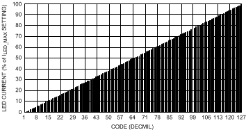 Figure 35. Linear Brightness Mapping
Table 3. ILED vs. Brightness Register Data (Linear Mapping)
| BRT DATA (HEX) | % FULL-SCALE CURRENT (LINEAR) | BRT DATA (HEX) | % OF FULL-SCALE CURRENT (LINEAR) | BRT DATA (HEX) | % OF FULL-SCALE CURRENT (LINEAR) | BRT DATA (HEX) | % OF FULL-SCALE CURRENT (LINEAR) |
|---|---|---|---|---|---|---|---|
| 0x00 | 0.00% | 0x20 | 25.79% | 0x40 | 50.78% | 0x60 | 75.78% |
| 0x01 | 1.57% | 0x21 | 26.57% | 0x41 | 51.57% | 0x61 | 76.56% |
| 0x02 | 2.35% | 0x22 | 27.35% | 0x42 | 52.35% | 0x62 | 77.35% |
| 0x03 | 3.13% | 0x23 | 28.13% | 0x43 | 53.13% | 0x63 | 78.13% |
| 0x04 | 3.91% | 0x24 | 28.91% | 0x44 | 53.91% | 0x64 | 78.91% |
| 0x05 | 4.69% | 0x25 | 29.69% | 0x45 | 54.69% | 0x65 | 79.69% |
| 0x06 | 5.48% | 0x26 | 30.47% | 0x46 | 55.47% | 0x66 | 80.47% |
| 0x07 | 6.26% | 0x27 | 31.25% | 0x47 | 56.25% | 0x67 | 81.25% |
| 0x08 | 7.04% | 0x28 | 32.04% | 0x48 | 57.03% | 0x68 | 82.03% |
| 0x09 | 7.82% | 0x29 | 32.82% | 0x49 | 57.82% | 0x69 | 82.81% |
| 0x0A | 8.60% | 0x2A | 33.60% | 0x4A | 58.60% | 0x6A | 83.59% |
| 0x0B | 9.38% | 0x2B | 34.38% | 0x4B | 59.38% | 0x6B | 84.38% |
| 0x0C | 10.16% | 0x2C | 35.16% | 0x4C | 60.16% | 0x6C | 85.16% |
| 0x0D | 10.94% | 0x2D | 35.94% | 0x4D | 60.94% | 0x6D | 85.94% |
| 0x0E | 11.72% | 0x2E | 36.72% | 0x4E | 61.72% | 0x6E | 86.72% |
| 0x0F | 12.51% | 0x2F | 37.50% | 0x4F | 62.50% | 0x6F | 87.50% |
| 0x10 | 13.29% | 0x30 | 38.29% | 0x50 | 63.28% | 0x70 | 88.28% |
| 0x11 | 14.07% | 0x31 | 39.07% | 0x51 | 64.06% | 0x71 | 89.06% |
| 0x12 | 14.85% | 0x32 | 39.85% | 0x52 | 64.85% | 0x72 | 89.84% |
| 0x13 | 15.63% | 0x33 | 40.63% | 0x53 | 65.63% | 0x73 | 90.63% |
| 0x14 | 16.41% | 0x34 | 41.41% | 0x54 | 66.41% | 0x74 | 91.41% |
| 0x15 | 17.19% | 0x35 | 42.19% | 0x55 | 67.19% | 0x75 | 92.19% |
| 0x16 | 17.97% | 0x36 | 42.97% | 0x56 | 67.97% | 0x76 | 92.97% |
| 0x17 | 18.76% | 0x37 | 43.75% | 0x57 | 68.75% | 0x77 | 93.75% |
| 0x18 | 19.54% | 0x38 | 44.53% | 0x58 | 69.53% | 0x78 | 94.53% |
| 0x19 | 20.32% | 0x39 | 45.32% | 0x59 | 70.39% | 0x79 | 95.31% |
| 0x1A | 21.10% | 0x3A | 46.10% | 0x5A | 71.10% | 0x7A | 96.09% |
| 0x1B | 21.88% | 0x3B | 46.88% | 0x5B | 71.88% | 0x7B | 96.88% |
| 0x1C | 22.66% | 0x3C | 47.66% | 0x5C | 72.66% | 0x7C | 97.66% |
| 0x1D | 23.44% | 0x3D | 48.44% | 0x5D | 73.44% | 0x7D | 98.44% |
| 0x1E | 24.22% | 0x3E | 49.22% | 0x5E | 74.22% | 0x7E | 99.22% |
| 0x1F | 25.00% | 0x3F | 50.00% | 0x5F | 75.00% | 0x7F | 100.00% |
NOTE
When determining the LED current from (Table 2 and Table 3 ) there is a typical offset of 113 µA with a ±300-µA variation that must be added to the calculated value for codes 0x0A and below. For example, in linear mode with IFULL_SCALE = 19 mA and brightness code 0x09 chosen, the nominal current setting is 0.0782 × 19 mA = 1.4858 mA. Adding in the 113-µA typical offset gives 1.4858 mA + 0.113 mA = 1.5988 mA. With the typical ±300-µA range, the high and low currents can be ILOW = 1.2988 mA, IHIGH = 1.8988 mA. For exponential mode with codes 0x0A and below, this offset and variation error gets divided down by 10 (11.3 µA offset with ±30-µA typical range).
8.3.13 Simple Enable Disable With PWM Current Control
With bits [7 and 5] of the General Configuration Register set to ‘1’ the PWM input is enabled as a simple enable/disable. The simple enable/disable feature operates as described in Figure 36. In this mode, when the PWM input is held high (PWM Polarity bit = 0) for > 2 ms the LM3530 will turn on the LED current at the programmed Full-Scale Current × % of Full-Scale Current as set by the code in the Brightness Control Register. When the PWM input is held low for > 2 ms the device will shut down. With the PWM Polarity bit = 1 the PWM input is configured for active low operation. In this configuration holding PWM low for > 2 ms will turn on the device at the programmed Full-Scale Current × % of Full-Scale Current as set by the code in the Brightness Control Register. Likewise, holding PWM high for > 2 ms will put the device in shutdown.
Driving the PWM input with a pulsed waveform at a variable duty cycle is also possible in simple enable/Disable mode, so long as the low pulse width is < 2 ms. When a PWM signal is used in this mode the input duty cycle information is internally filtered, and an analog voltage is used to control the LED current. This type of PWM control (PWM to Analog current control) prevents large voltage excursions across the output capacitor that can result in audible noise. Simple Enable/Disable mode can be useful since the default bit setting for the General Configuration Register is 0xCC (Simple Enable bit = 1, PWM Enable = 1, and Full-Scale Current = 19mA). Additionally, the default Brightness Register setting is 0x7F (100% of Full-Scale current). This gives the LM3530 the ability to turn on after power up (or after reset) without having to do any writes to the I2C-compatible bus.
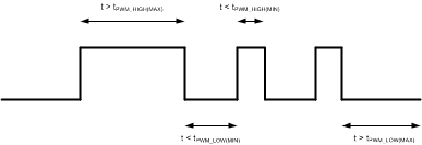 Figure 36. Simple Enable/Disable Timing
Example: Simple Enable Disable with PWM Current Control):
As an example, assume that the HWEN input is toggled low then high. This resets the LM3530 and sets all the registers to their default value. When the PWM input is then pulled high for > 2 ms the LED current becomes:

where
- BRT is the % of ILED_FS as set in the Brightness Control Register.
If then the PWM input is fed with a 5-kHz pulsed waveform at 40% duty cycle the LED current becomes:

Then, if the Brightness Control Register is loaded with 0x55 (9.6% of Full-Scale Current) the LED current becomes:

8.3.14 Ambient Light Current Control
With bits [4:3] of the ALS Configuration Register both set to 1, the LM3530 is configured for Ambient Light Current Control. In this mode the ambient light sensing inputs (ALS1, and/or ALS2) monitor the outputs of analog output ambient light sensing photo diodes and adjust the LED current depending on the ambient light. The ambient light sensing circuit has 4 configurable Ambient Light Boundaries (ZB0 – ZB3) programmed through the four (8-bit) Zone Boundary Registers. These zone boundaries define 5 ambient brightness zones (Figure 27). Each zone corresponds to a programmable brightness setting which is programmable through the 5 Zone Target Registers (Z0T – Z4T). When the ALS1, and/or ALS2 input (depending on the bit settings of the ALS Input Select bits) detects that the ambient light has crossed to a new zone (as defined by one of the Zone Boundary Registers) the LED current becomes a function of the Brightness Code loaded in the Zone Target Register which corresponds to the new ambient light brightness zone.
On start-up the 4 Zone Boundary Registers are pre-loaded with 0x33 (51d), 0x66 (102d), 0x99 (153d), and 0xCC (204d). Each ALS input has a 1-V active input voltage range with a 4mV offset voltage which makes the default Zone Boundaries set at:
Zone Boundary 0 = 1V × 51/255 + 4 mV = 204 mV
Zone Boundary 1 = 1V × 102/255 + 4 mV = 404 mV
Zone Boundary 2 = 1V × 153/255 + 4 mV = 604 mV
Zone Boundary 3 = 1V × 204/255 + 4 mV = 804 mV
These Zone Boundary Registers are all 8-bit (readable and writable) registers. The first zone (Z0) is defined between 0 and 204 mV, the Z1 default is defined between 204 mV and 404 mV, the Z2 default is defined between 404 mV and 604 mV, the Z3 default is defined between 604 mV and 804 mV, and the Z4 default is defined between 804 mV and 1.004 V. The default settings for the 5 Zone Target Registers are 0x19, 0x33, 0x4C, 0x66, and 0x7F. This corresponds to LED brightness settings of 0.336%, 1.43%, 5.781%, 24.844%, and 100% of full-scale current respectively (assuming exponential backlight mapping).
Example: Ambient Light Control Current:
As an example, assume that the APDS-9005 is used as the ambient light sensing photo diode with its output connected to the ALS1 input. The ALS Resistor Select Register is loaded with 0x04 which configures the ALS1 input for a 2.27-kΩ internal pull-down resistor (see Table 9). The APDS-9005 has a typical 400nA/LUX response. With a 2.27-kΩ resistor the sensor output would see a 0-mV to 908-mV swing with a 0 to 1000 LUX change in ambient light. Next, the ALS Configuration Register is programmed with 0x3C. From Table 6, this configures the LM3530’s ambient light sensing interface for:
ALS1 as the active ALS input (bits [6:5] = 01)
Ambient Light Current Control Enabled (bit 4 = 1)
ALS circuitry Enabled (bit 3 = 1)
Sets the ALS Averaging Time to 512 ms (bits [2:0] = 100)
Next, the General Configuration Register is programmed with 0x19 which sets the Full-Scale Current to 26 mA, selects Exponential Brightness Mapping, and enables the device via the I2C-compatible interface.
Now assume that the APDS-9005 ambient light sensor detects a 100 LUX ambient light at its input. This forces the ambient light sensors output (and the ALS1 input) to 87.5mV corresponding to Zone 0. Since Zone 0 points to the brightness code programmed in Zone Target Register 0 (loaded with code 0x19), the LED current becomes:

Where the code in Zone Target Register 0 points to the % of ILED_FS as given by Table 2 or Table 3, depending on whether Exponential or Linear Mapping are selected.
Next, assume that the ambient light changes to 500 LUX (corresponding to an ALS1 voltage of 454 mV). This moves the ambient light into Zone 2 which corresponds to Zone Target Register 2 (loaded with code 0x4C) the LED current then becomes:

8.3.15 Ambient Light Current Control + PWM
The Ambient Light Current Control can also be a function of the PWM input duty cycle. Assume the LM3530 is configured as described in the above Ambient Light Current Control example, but this time the Enable PWM bit set to ‘1’ (General Configuration Register bit [5]).
Example: Ambient Light Current Control + PWM
In this example, the APDS-9005 detects that the ambient light has changed to 1 kLUX. The voltage at ALS1 is now around 908 mV, and the ambient light falls within Zone 5. This causes the LED brightness to be a function of Zone Target Register 5 (loaded with 0x7F). Now assume the PWM input is also driven with a 50% duty cycle pulsed waveform. The LED current now becomes:

Example: ALS Averaging:
As an example, suppose the LM3530 ALS Configuration Register is loaded with 0x3B. This configures the device for:
ALS1 as the active ALS input (bits [6:5] = 01)
Enables Ambient Light Current Control (bit 4 = 1)
Enables the ALS circuitry (bit 3 = 1)
Sets the ALS Averaging Time to 256 ms (bits [2:0] = 011)
Next, the ALS Resistor Select Register is loaded with 0x04. This configures the ALS2 input as high impedance and configures the ALS1 input with a 2.27-kΩ internal pull-down resistor. The Zone Boundary Registers and Zone Target Registers are left with their default values. The Brightness Ramp Rate Register is loaded with 0x2D. This sets up the LED current ramp rate at 16.384 ms/step. Finally, the General Configuration Register is loaded with 0x15. This sets up the device with:
Simple Enable OFF (bit 7 = 0)
PWM Polarity High (bit 6 = 0)
PWM Input Disabled (bit 5 = 0)
Full-Scale Current = 22.5mA (bits [4:2] = 101)
Brightness Mapping Mode as Exponential (bit 1 = 0)
Device Enabled via I2C (bit 0 = 1)
As the device starts up the APDS-9005 ambient light sensor (connected to the ALS1 input) detects 500 LUX. This puts approximately 437.5 mV at ALS1 (see Figure 37). This places the measured ambient light between Zone Boundary Registers 1 and 2, thus corresponding to Zone Target Register 2. The default value for this register is 0x4C. The LED current is programmed to:

Referring to Figure 37, initially the Averager is loaded with Zone 0 so it takes 2 averaging periods for the LM3530 to change to the new zone. After the ALS1 voltage remains at 437.5 mV for two averaging periods (end of period 2) the LM3530 repeats Zone 2 and signals the LED current to begin ramping to the Zone 2 target beginning at average period 3. Since the ramp rate is set at 16.384 ms/step the LED current goes from 0 to 1.3 mA in 76 × 16.384 ms = 1.245s (approximately 5 average periods).
After the LED current has been at its steady state of 1.3 mA for a while, the ambient light suddenly steps to 900 LUX for 500 ms and then steps back to 500 LUX. In this case the 900 LUX will place the ALS1 voltage at approximately 979 mV corresponding to Zone 4 somewhere during average period 10 and fall back to 437.5 mV somewhere during average period 12. The averager output during period #10 goes to 3, and then during period 11, goes to 4. Since there have been 2 increases in the average during period 10 and period 11, the beginning of average period #12 shows a change in the brightness zone to Zone 4. This results in the LED current ramping to the new value of 22.5 mA (the Zone 4 target). During period #12 the ambient light steps back to 500 LUX and forces ALS1 to 437.5 mV (corresponding to Zone 2). After average period 12 and period 13 have shown that the averager transitioned lower two times, the brightness zone changes to the new target at the beginning of period 14. This signals the LED current to ramp down to the zone 2 target of 1.3 mA. Looking back at average period 12 and period 13, the LED current was only able to ramp up to 7.38 mA due to the ramp rate of 16.384 ms/step (2 average periods of 256 ms each) before it was instructed to ramp back to the Zone 2 target at the start of period 14. This example demonstrates not only the averaging feature, but how additional filtering of transient events on the ALS inputs can be accomplished by using the LED current ramp rates.
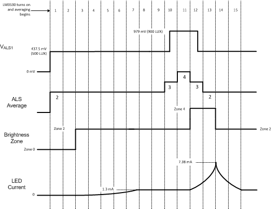 Figure 37. ALS Averaging Example
8.3.16 Interrupt Output
INT is an open-drain output which pulls low when the Ambient Light Sensing circuit has transitioned to a new ambient brightness zone. When a read-back of the ALS Information Register is done INT is reset to the open drain state.
8.3.17 Overvoltage Protection
Overvoltage protection is set at 40 V (minimum) for the LM3530-40 and 23.6 V minimum for the LM3530-25. The 40-V version allows typically up to 11 series white LEDs (assuming 3.5 V per LED + 400 mV headroom voltage for the current sink = 38.9 V). When the OVP threshold is reached the LM3530 switching converter stops switching, allowing the output voltage to discharge. Switching will resume when the output voltage falls to typically 1 V below the OVP threshold. In the event of an LED open circuit the output will be limited to around 40 V with a small amount of voltage ripple. The 25-V version allows up to 6 series white LEDs (assuming 3.5-V per LED + 400 mV headroom voltage for the current sink = 21.4 V). The 25-V OVP option allows for the use of lower voltage and smaller sized (25 V) output capacitors. The 40-V device would typically require a 50-V output capacitor.
8.3.18 Hardware Enable
The HWEN input is an active high hardware enable which must be pulled high to enable the device. Pulling this pin low disables the I2C-compatible interface, the simple enable/disable input, the PWM input, and resets all registers to their default state (see Table 4).
8.3.19 Thermal Shutdown
In the event the die temperature reaches 140°C, the LM3530 will stop switching until the die temperature cools by 15°C. In a thermal shutdown event the device is not placed in reset; therefore, the contents of the registers are left in their current state.
8.4 Device Functional Modes
8.4.1 Shutdown
With HWEN Low, or bit 0 in register 0x10 set to 0, the device is in shutdown. In this mode the boost converter and the current sink are both off and the supply current into IN is reduced to typically 1 µA.
8.4.2 I2C Mode
I2C-Compatible Control Mode is enabled by writing a '1' to the I2C Device Enable bit (bit [0] of the General Configuration Register), a '0' to the Simple Enable bit (bit 7), and a '0' to the PWM Enable bit (bit 5). With bit 5 = 0, the duty cycle information at the PWM input is not used in setting the LED current. In this mode the LED current is a function of the Full-Scale LED current bits (bits [4:2] of the General Configuration Register) and the code in the Brightness Control Register. The LED current mapping for the Brightness Control Register can be linear or exponential depending on bit [1] in the General Configuration Register (see Exponential or Linear Brightness Mapping Modes section). Using I2C-Compatible Control Only, the Full-Scale LED Current bits and the Brightness Control Register code provides nearly 1016 possible current levels selectable over the I2C-compatible interface.
8.4.3 PWM + I2C Mode
PWM + I2C-compatible current control mode is enabled by writing a ‘1’ to the Enable PWM bit (General Configuration Register bit [5]) and writing a ‘1’ to the I2C Device Enable bit (General Configuration Register bit 0). This makes the LED current a function of the PWM input duty cycle (D), the Full-Scale LED current (ILED_FS), and the % of full-scale LED current . The % of Full-Scale LED current is set by the code in the Brightness Control Register. The LED current using PWM + I2C-Compatible Control is given by Equation 11:

BRT is the percentage of Full Scale Current as set in the Brightness Control Register. The Brightness Control Register can have either exponential or linear brightness mapping depending on the setting of the BMM bit (bit [1] in General Configuration Register).
8.4.4 ALS Mode
With bits [4:3] of the ALS Configuration Register both set to 1, the LM3530 is configured for Ambient Light Current Control. In this mode the ambient light sensing inputs (ALS1, and/or ALS2) monitor the outputs of analog output ambient light sensing photo diodes and adjust the LED current depending on the ambient light.
8.4.5 Simple Enable Mode
Simple Enable Mode With bits [7 and 5] of the General Configuration Register set to ‘1’ the PWM input is enabled as a simple enable/disable. The simple enable/disable feature operates as described in Figure 36. In this mode, when the PWM input is held high (PWM Polarity bit = 0) for > 2 ms the LM3530 will turn on the LED current at the programmed Full-Scale Current × % of Full-Scale Current as set by the code in the Brightness Control Register. When the PWM input is held low for > 2 ms the device will shut down.
8.5 Programming
8.5.1 I2C-Compatible Interface
8.5.1.1 Start and Stop Condition
The LM3530 is controlled via an I2C-compatible interface. START and STOP conditions classify the beginning and the end of the I2C session. A START condition is defined as SDA transitioning from HIGH to LOW while SCL is HIGH. A STOP condition is defined as SDA transitioning from LOW to HIGH while SCL is HIGH. The I2C master always generates the START and STOP conditions. The I2C bus is considered busy after a START condition and free after a STOP condition. During data transmission, the I2C master can generate repeated START conditions. A START and a repeated START conditions are equivalent function-wise. The data on SDA must be stable during the HIGH period of the clock signal (SCL). In other words, the state of SDA can only be changed when SCL is LOW.
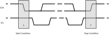 Figure 38. Start and Stop Sequences
8.5.1.2 I2C-Compatible Address
The 7bit chip address for the LM3530 is (0x38, or 0x39) for the 40-V version and (0x36) for the 25-V version. After the START condition, the IC master sends the 7-bit chip address followed by an eighth bit (LSB) read or write (R/W). R/W= 0 indicates a WRITE and R/W = 1 indicates a READ2. The second byte following the chip address selects the register address to which the data will be written. The third byte contains the data for the selected register.
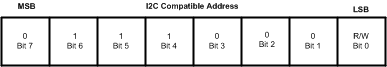 Figure 39. I2C-Compatible Chip Address (0x38)
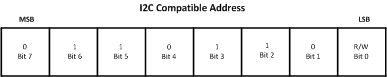 Figure 40. I2C-Compatible Chip Address (0x36)
8.5.1.3 Transferring Data
Every byte on the SDA line must be eight bits long, with the most significant bit (MSB) transferred first. Each byte of data must be followed by an acknowledge bit (ACK). The acknowledge related clock pulse (9th clock pulse) is generated by the master. The master then releases SDA (HIGH) during the 9th clock pulse. The LM3530 pulls down SDA during the 9th clock pulse, signifying an acknowledge. An acknowledge is generated after each byte has been received.
There are fourteen 8-bit registers within the LM3530 as detailed in Table 4.
8.6 Register Maps
8.6.1 Register Descriptions
Table 4. LM3530 Register Definition
| REGISTER NAME | FUNCTION | ADDRESS | POR VALUE |
|---|---|---|---|
| General Configuration | 1. Simple Interface Enable 2. PWM Polarity 3. PWM enable 4. Full-Scale Current Selection 5. Brightness Mapping Mode Select 6. I2C Device Enable |
0x10 | 0xB0 |
| ALS Configuration | 1. ALS Current Control Enable 2. ALS Input Enable 3. ALS Input Select 4. ALS Averaging Times |
0x20 | 0x2C |
| Brightness Ramp Rate | Programs the rate of rise and fall of the LED current | 0x30 | 0x00 |
| ALS Zone Information | 1. Zone Boundary Change Flag 2. Zone Brightness Information |
0x40 | 0x00 |
| ALS Resistor Select | Internal ALS1 and ALS2 Resistances | 0x41 | 0x00 |
| Brightness Control (BRT) | Holds the 7 bit Brightness Data | 0xA0 | 0x7F |
| Zone Boundary 0 (ZB0) | ALS Zone Boundary #0 | 0x60 | 0x33 |
| Zone Boundary 1 (ZB1) | ALS Zone Boundary #1 | 0x61 | 0x66 |
| Zone Boundary 2 (ZB2) | ALS Zone Boundary #2 | 0x62 | 0x99 |
| Zone Boundary 3 (ZB3) | ALS Zone Boundary #3 | 0x63 | 0xCC |
| Zone Target 0 (Z0T) | Zone 0 LED Current Data. The LED Current Source transitions to the brightness code in Z0T when the ALS_ input is less than the zone boundary programmed in ZB0. | 0x70 | 0x19 |
| Zone Target 1 (Z1T) | Zone 1 LED Current Data. The LED Current Source transitions to the brightness code in Z1T when the ALS_ input is between the zone boundaries programmed in ZB1 and ZB0. | 0x71 | 0x33 |
| Zone Target 2 (Z2T) | Zone 2 LED Current Data. The LED Current Source transitions to the brightness code in Z2T when the ALS_ input is between the zone boundaries programmed in ZB2 and ZB1. | 0x72 | 0x4C |
| Zone Target 3 (Z3T) | Zone 3 LED Current Data. The LED Current Source transitions to the brightness code in Z3T when the ALS_ input is between the zone boundaries programmed in ZB3 and ZB2. | 0x73 | 0x66 |
| Zone Target 4 (Z4T) | Zone 4 LED Current Data. The LED Current Source transitions to the brightness code in Z4T when the ALS_ input is between the zone boundaries programmed in ZB4 and ZB3. | 0x74 | 0x7F |
*Note: Unused bits in the LM3530 Registers default to a logic '1'.
8.6.1.1 General Configuration Register (GP)
The General Configuration Register (address 0x10) is described in Figure 41 and Table 5.
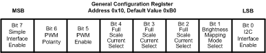 Figure 41. General Configuration Register
Table 5. General Configuration Register Description (0x10)
| Bit 7 (PWM Simple Enable |
Bit 6 (PWM Polarity) |
Bit 5 (EN_PWM) see Figure 31 |
Bit 4 (Full-Scale Current Select) |
Bit 3 (Full-Scale Current Select) |
Bit 2 (Full-Scale Current Select) |
Bit 1 (Mapping Mode Select) |
Bit 0 (I2C Device Enable) |
|---|---|---|---|---|---|---|---|
| 0 = Simple Interface at PWM Input is Disabled 1 = Simple Interface at PWM Input is Enabled |
0 = PWM active high 1 = PWM active low |
0 = LED current is not a function of PWM duty cycle 1 = LED current is a function of duty cycle |
000 = 5 mA full-scale current 001 = 8.5 mA full-scale current 010 = 12 mA full-scale current 011 = 15.5 mA full-scale current 100 = 19 mA full-scale current 101 = 22.5 mA full-scale current 110 = 26 mA full-scale current 111 = 29.5 mA full-scale current |
0 = exponential mapping 1 = linear mapping |
0 = Device Disabled 1 = Device Enabled |
||
8.6.1.2 ALS Configuration Register
The ALS Configuration Register controls the Ambient Light Sensing input functions and is described in Figure 42 and Table 6.
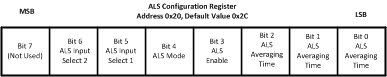 Figure 42. ALS Configuration Register
Table 6. ALS Configuration Register Description (0x20)
| Bit 7 | Bit 6 ALS Input Select |
Bit 5 ALS Input Select |
Bit 4 ALS Enable |
Bit 3 ALS Enable |
Bit 2 ALS Averaging Time |
Bit 1 ALS Averaging Time |
Bit 0 ALS Averaging Time |
|---|---|---|---|---|---|---|---|
| N/A | 00 = The Average of ALS1 and ALS2 is used to control the LED brightness 01 = ALS1 is used to control the LED brightness 10 = ALS2 is used to control the LED brightness 11 = The ALS input with the highest voltage is used to control the LED brightness |
00 or 10 = ALS is disabled. The Brightness Register is used to determine the LED current. 01 = ALS is enabled. The Brightness Register is used to determine the LED Current. 11 = ALS inputs are enabled. Ambient light determines the LED current. |
000 = 32 ms 001 = 64 ms 010 = 128 ms 011 = 256 ms 100 = 512 ms 101 = 1024 ms 110 = 2048 ms 111 = 4096 ms |
||||
8.6.1.3 Brightness Ramp Rate Register
The Brightness Ramp Rate Register controls the rate of rise or fall of the LED current. Both the rising rate and falling rate are independently adjustable Figure 43 and Table 7 describe the bit settings.
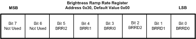 Figure 43. Brightness Ramp Rate Register
Table 7. Brightness Ramp Rate Register Description (0x30)
| Bit 7 | Bit 6 | Bit 5 (BRRI2) |
Bit 4 (BRRI1) |
Bit 3 (BRRI0) |
Bit 2 (BRRD2) |
Bit 1 (BRRD1) |
Bit 0 (BRRD0) |
|---|---|---|---|---|---|---|---|
| N/A | N/A | 000 = 8 µs/step (1.106 ms from 0 to Full Scale) 001 = 1.024 ms/step (130 ms from 0 to Full Scale) 010 = 2.048 ms/step (260 ms from 0 to Full Scale) 011 = 4.096 ms/step (520 ms from 0 to Full Scale) 100 = 8.192 ms/step (1.04 s from 0 to Full Scale) 101 = 16.384 ms/step (2.08 s from 0 to Full Scale) 110 = 32.768 ms/step (4.16 s from 0 to Full Scale) 111 = 65.538 ms/step (8.32 s from 0 to Full Scale) |
000 = 8 µs/step (1.106 ms from Full Scale to 0) 001 = 1.024 ms/step (130 ms from Full Scale to 0) 010 = 2.048 ms/step (260 ms from Full Scale to 0) 011 = 4.096 ms/step (520 ms from Full Scale to 0) 100 = 8.192 ms/step (1.04 s from Full Scale to 0) 101 = 16.384 ms/step (2.08 s from Full Scale to 0) 110 = 32.768 ms/step (4.16 s from Full Scale to 0) 111 = 65.538 ms/step (8.32 s from Full Scale to 0) |
||||
8.6.1.4 ALS Zone Information Register
The ALS Zone Information Register is a read-only register that is updated every time the active ALS input(s) detect that the ambient light has changed to a new zone as programmed in the Zone Boundary Registers. See Zone Boundary Register description. A new update to the ALS Zone Information Register is signaled by the INT output going from high to low. A read-back of the ALS Zone Information Register will cause the INT output to go open-drain again. The Zone Change Flag (bit 3) is also updated on a Zone change and cleared on a read back of the ALS Zone Information Register. Figure 44 and Table 8 detail the ALS Zone Information Register.
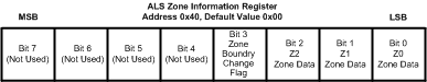 Figure 44. ALS Zone Information Register
Table 8. ALS Zone Information Register Description (0x40)
| Bit 7 | Bit 6 | Bit 5 | Bit 4 | Bit 3 (Zone Boundary Change Flag) |
Bit 2 (Z2) |
Bit 1 (Z1) |
Bit 0 (Z0) |
|---|---|---|---|---|---|---|---|
| N/A | N/A | N/A | N/A | 1 = the active ALS input has changed to a new ambient light zone as programmed in the Zone Boundary Registers (ZB0 -ZB3) 0 = no zone change |
000 = Zone 0 001 = Zone 1 010 = Zone 2 011 = Zone 3 100 = Zone 4 |
||
8.6.1.5 ALS Resistor Select Register
The ALS Resistor Select Register configures the internal resistance from either the ALS1 or ALS2 input to GND. Bits [3:0] program the input resistance at the ALS1 input and bits [7:4] program the input resistance at the ALS2 input. With bits [3:0] set to all zeroes the ALS1 input is high impedance. With bits [7:4] set to all zeroes the ALS2 input is high impedance.
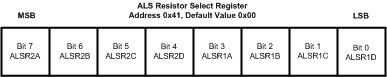 Figure 45. ALS Resistor Select Register
Table 9. ALS Resistor Select Register Description (0x41)
| Bit 7 (ALSR2A) |
Bit 6 (ALSR2B) |
Bit 5 (ALSR2C) |
Bit 4 (ALSR2D) |
Bit 3 (ALSR1A) |
Bit 2 (ALSR1B) |
Bit 1 (ALSR1C) |
Bit 0 (ALSR1D) |
|---|---|---|---|---|---|---|---|
| 0000 = ALS2 is high impedance 0001 = 13.531 kΩ (73.9 µA at 1 V) 0010 = 9.011 kΩ (111 µA at 1 V) 0011 = 5.4116 kΩ (185 µA at 1 V) 0100 = 2.271 kΩ (440 µA at 1 V) 0101 = 1.946 kΩ (514 µA at 1 V) 0110 = 1.815 kΩ (551 µA at 1 V) 0111 = 1.6 kΩ (625 µA at 1 V) 1000 = 1.138 kΩ (879 µA at 1 V) 1001 = 1.05 kΩ (952 µA at 1 V) 1010 = 1.011 kΩ (989 µA at 1 V) 1011 = 941 Ω (1.063 mA at 1 V) 1100 = 759 Ω (1.318 mA at 1 V) 1101 = 719 Ω (1.391 mA at 1 V) 1110 = 700 Ω (1.429 mA at 1 V) 1111 = 667 Ω (1.499 mA at 1 V) |
0000 = ALS2 is high impedance 0001 = 13.531 kΩ (73.9 µA at 1 V) 0010 =9.011 kΩ (111 µA at 1 V) 0011 = 5.4116 kΩ (185 µA at 1 V) 0100 = 2.271 kΩ (440 µA at 1 V) 0101 = 1.946 kΩ (514 µA at 1 V) 0110 = 1.815 kΩ (551 µA at 1 V) 0111 = 1.6 kΩ (625 µA at 1 V) 1000 = 1.138 kΩ (879µA at 1 V) 1001 = 1.05 kΩ (952 µA at 1 V) 1010 = 1.011 kΩ (989 µA at 1 V) 1011 = 941 Ω (1.063 mA at 1 V) 1100 = 759 Ω (1.318 mA at 1 V) 1101 = 719 Ω (1.391 mA at 1 V) 1110 = 700 Ω (1.429 mA at 1 V) 1111 = 667 Ω (1.499 mA at 1 V) |
||||||
8.6.1.6 Brightness Control Register
The Brightness Register (BRT) is an 8-bit register that programs the 127 different LED current levels (Bits [6:0]). The code written to BRT is translated into an LED current as a percentage of ILED_FULLSCALE as set via the Full-Scale Current Select bits (General Configuration Register bits [4:2]). The LED current response has a typical 1000:1 dimming ratio at the maximum full-scale current (General Configuration Register bits [4:2] = (111) and using the exponential weighted dimming curve.
There are two selectable LED current profiles. Setting the General Configuration Register bit 1 to 0 selects the exponentially weighted LED current response (see Figure 34). Setting this bit to '1' selects the linear weighted curve (see Figure 35). Table 2 and Table 3 show the percentage Full-Scale LED Current at a given Brightness Register Code for both the Exponential and Linear current response.
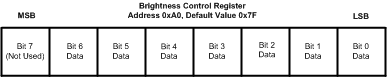 Figure 46. Brightness Control Register
Table 10. Brightness Control Register Description (0xA0)
| Bit 7 N/A |
Bit 6 Data (MSB) |
Bit 5 Data |
Bit 4 Data |
Bit 3 Data |
Bit 2 Data |
Bit 1 Data |
Bit 0 Data |
|---|---|---|---|---|---|---|---|
| LED Brightness Data (Bits [6:0] | |||||||
| Exponential Mapping (see Table 2) 0000000 = LEDs Off 0000001 = 0.08% of Full Scale : : : 1111111 = 100% of Full Scale |
Linear Mapping (see Table 3) 0000000 = LEDs Off 0000001 = 0.79% of Full Scale : : : 1111111 = 100% of Full Scale |
||||||
8.6.1.7 Zone Boundary Register
The Zone Boundary Registers are programmed with the ambient light sensing zone boundaries. The default values are set at 20% (200 mV), 40% (400 mV), 60% (600 mV), and 80% (800 mV) of the full-scale ALS input voltage range (1V). The necessary conditions for proper ALS operation are that the data in ZB0 < data in ZB1 < data in ZB2 < data in ZB3.
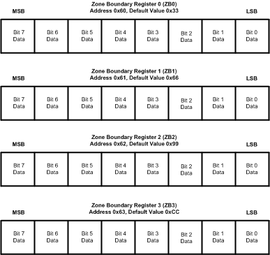 Figure 47. Zone Boundary Registers
8.6.1.8 Zone Target Registers
The Zone Target Registers contain the LED brightness data that corresponds to the current active ALS zone. The default values for these registers and their corresponding percentage of full-scale current for both linear and exponential brightness is shown in Figure 48 and Table 11.
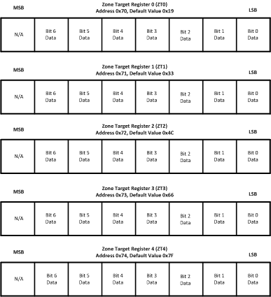 Figure 48. Zone Target Registers
Table 11. Zone Boundary and Zone Target Default Mapping
| ZONE BOUNDARY (DEFAULT) |
ZONE TARGET REGISTER (DEFAULT) | FULL-SCALE CURRENT (DEFAULT) | LINEAR MAPPING (DEFAULT) | EXPONENTIAL MAPPING (DEFAULT) |
|---|---|---|---|---|
| Boundary 0, Active ALS input is less than 200 mV |
0x19 | 19 mA | 19.69% (3.74 µA) | 0.336% (68.4 µA) |
| Boundary 1, Active ALS input is between 200 mV and 400 mV |
0x33 | 19 mA | 40.16% (7.63 µA) | 1.43% (272 µA) |
| Boundary 2, Active ALS input is between 400 mV and 600 mV |
0x4C | 19 mA | 59.84% (11.37 mA) | 5.78% (1.098 mA) |
| Boundary 3, Active ALS input is between 600 mV and 800 mV |
0x66 | 19 mA | 80.31% (15.26 mA) | 24.84% (4.72 mA) |
| Boundary 4, Active ALS input is greater than 800mV |
0x7F | 19 mA | 100% (19 mA) | 100% (19 mA) |