SNVS606L June 2009 – December 2014 LM3530
PRODUCTION DATA.
- 1 Features
- 2 Applications
- 3 Description
- 4 Revision History
- 5 I2C Device Options
- 6 Pin Configuration and Functions
- 7 Specifications
-
8 Detailed Description
- 8.1 Overview
- 8.2 Functional Block Diagram
- 8.3
Feature Description
- 8.3.1 Start-Up
- 8.3.2 Light Load Operation
- 8.3.3 Ambient Light Sensor
- 8.3.4 ALS Operation
- 8.3.5 ALS Averaging Time
- 8.3.6 Zone Boundary Settings
- 8.3.7 Zone Boundary Trip Points and Hysteresis
- 8.3.8 Minimum Zone Boundary Settings
- 8.3.9 LED Current Control
- 8.3.10 Exponential or Linear Brightness Mapping Modes
- 8.3.11 PWM Input Polarity
- 8.3.12 I2C-Compatible Current Control Only
- 8.3.13 Simple Enable Disable With PWM Current Control
- 8.3.14 Ambient Light Current Control
- 8.3.15 Ambient Light Current Control + PWM
- 8.3.16 Interrupt Output
- 8.3.17 Overvoltage Protection
- 8.3.18 Hardware Enable
- 8.3.19 Thermal Shutdown
- 8.4 Device Functional Modes
- 8.5 Programming
- 8.6 Register Maps
- 9 Application and Implementation
- 10Power Supply Recommendations
- 11Layout
- 12Device and Documentation Support
- 13Mechanical, Packaging, and Orderable Information
Package Options
Mechanical Data (Package|Pins)
Thermal pad, mechanical data (Package|Pins)
Orderable Information
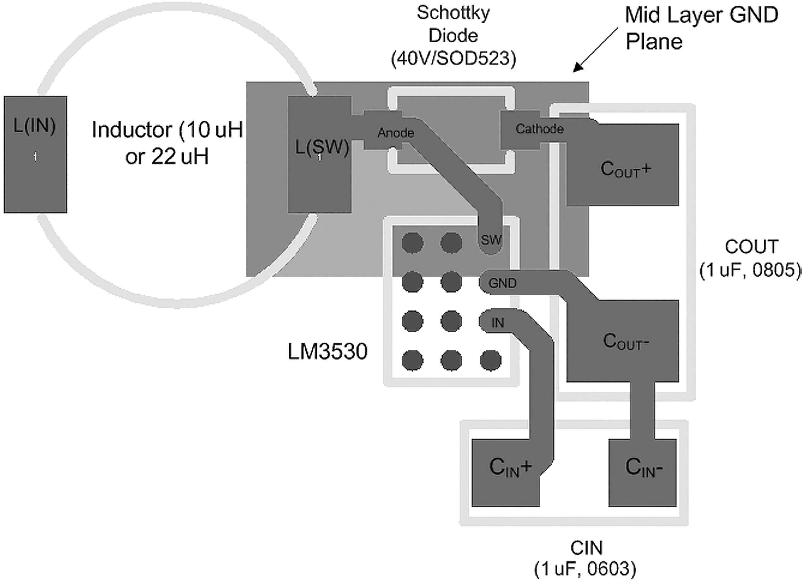
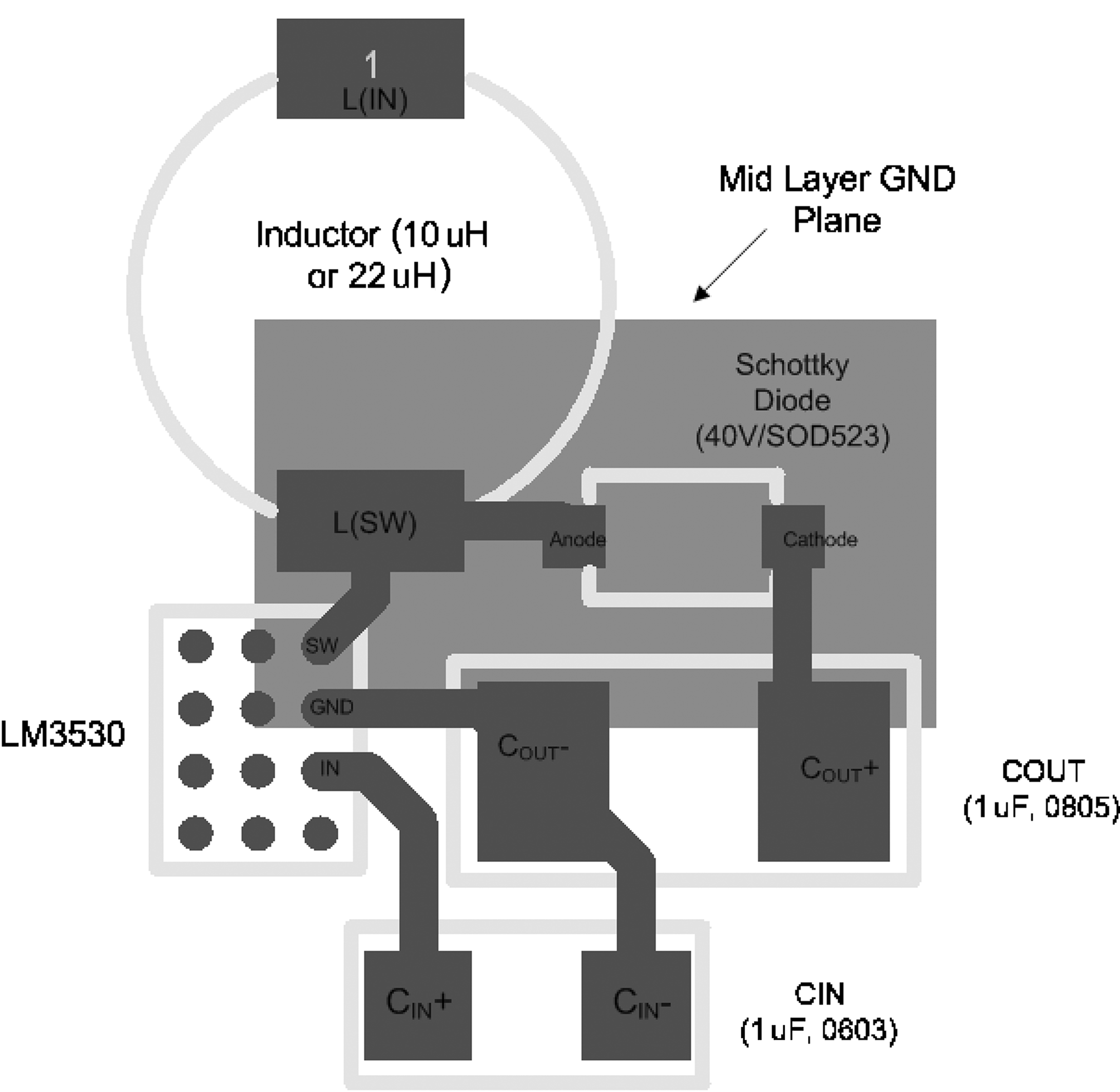
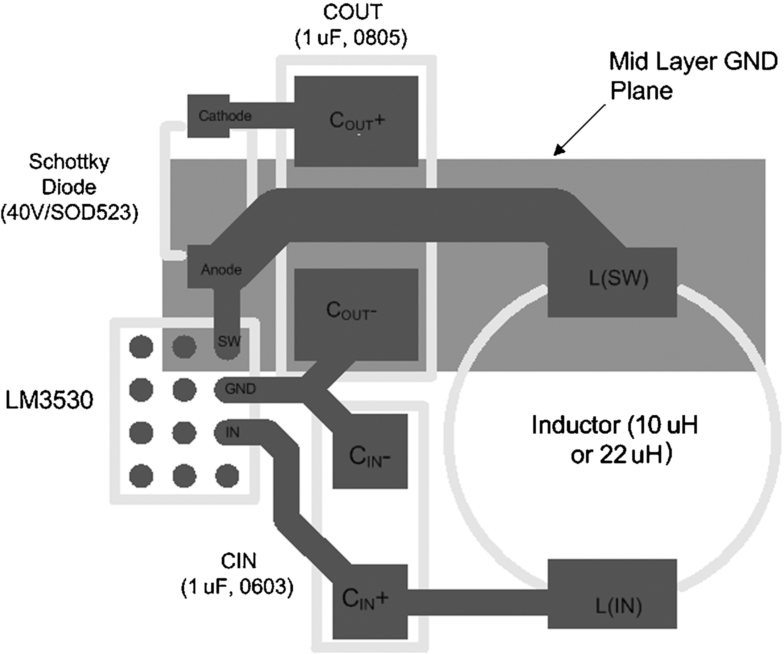
11 Layout
11.1 Layout Guidelines
The LM3530 contains an inductive boost converter which detects a high switched voltage (up to 40 V) at the SW pin, and a step current (up to 900 mA) through the Schottky diode and output capacitor each switching cycle. The high switching voltage can create interference into nearby nodes due to electric field coupling (I = CdV/dt). The large step current through the diode and the output capacitor can cause a large voltage spike at the SW pin and the OVP pin due to parasitic inductance in the step current conducting path (V = Ldi/dt). Board layout guidelines are geared towards minimizing this electric field coupling and conducted noise. Figure 56 highlights these two noise generating components.
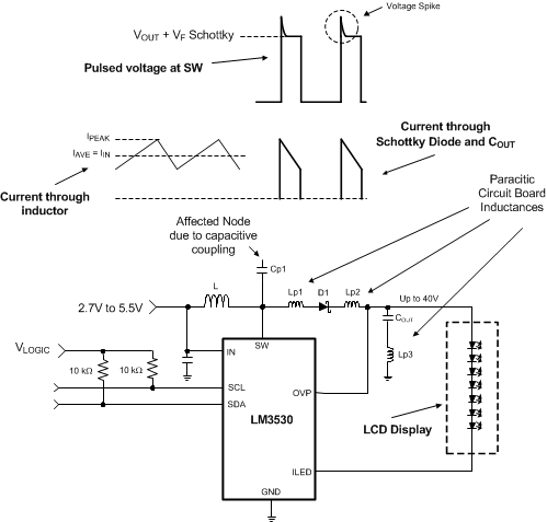 Figure 56. LM3530 Boost Converter Showing Pulsed Voltage At SW (High Dv/Dt) and
 Current Through Schottky and COUT (High Di/Dt)
The following lists the main (layout sensitive) areas of the LM3530 in order of decreasing importance:
- Output Capacitor
- Schottky Cathode to COUT+
- COUT– to GND
- Schottky Diode
- SW Pin to Schottky Anode
- Schottky Cathode to COUT+
- Inductor
- SW Node PCB capacitance to other traces
- Input Capacitor
- CIN+ to IN pin
- CIN– to GND
11.1.1 Output Capacitor Placement
The output capacitor is in the path of the inductor current discharge path. As a result COUT detects a high current step from 0 to IPEAK each time the switch turns off and the Schottky diode turns on. Any inductance along this series path from the cathode of the diode through COUT and back into the LM3530 GND pin will contribute to voltage spikes (VSPIKE = LP_ × dI/dt) at SW and OUT which can potentially overvoltage the SW pin, or feed through to GND. To avoid this, COUT+ must be connected as close as possible to the Cathode of the Schottky diode and COUT– must be connected as close as possible to the device GND bump. The best placement for COUT is on the same layer as the LM3530 so as to avoid any vias that can add excessive series inductance (see Figure 58, Figure 59, and Figure 60).
11.1.2 Schottky Diode Placement
The Schottky diode is in the path of the inductor current discharge. As a result the Schottky diode detects a high current step from 0 to IPEAK each time the switch turns off and the diode turns on. Any inductance in series with the diode will cause a voltage spike (VSPIKE = LP_ × dI/dt) at SW and OUT which can potentially overvoltage the SW pin, or feed through to VOUT and through the output capacitor and into GND. Connecting the anode of the diode as close as possible to the SW pin and the cathode of the diode as close as possible to COUT+ will reduce the inductance (LP_) and minimize these voltage spikes (see Figure 58, Figure 59, and Figure 60 ).
11.1.3 Inductor Placement
The node where the inductor connects to the LM3530 SW bump has 2 issues. First, a large switched voltage (0 to VOUT + VF_SCHOTTKY) appears on this node every switching cycle. This switched voltage can be capacitively coupled into nearby nodes. Second, there is a relatively large current (input current) on the traces connecting the input supply to the inductor and connecting the inductor to the SW bump. Any resistance in this path can cause large voltage drops that will negatively affect efficiency.
To reduce the capacitively coupled signal from SW into nearby traces, the SW bump to inductor connection must be minimized in area. This limits the PCB capacitance from SW to other traces. Additionally, the other traces need to be routed away from SW and not directly beneath. This is especially true for high impedance nodes that are more susceptible to capacitive coupling such as (SCL, SDA, HWEN, PWM, and possibly ASL1 and ALS2). A GND plane placed directly below SW will dramatically reduce the capacitive coupling from SW into nearby traces
To limit the trace resistance of the VBATT to inductor connection and from the inductor to SW connection, use short, wide traces (see Figure 58, Figure 59, and Figure 60).
11.1.4 Input Capacitor Selection and Placement
The input bypass capacitor filters the inductor current ripple, and the internal MOSFET driver currents during turn on of the power switch.
The driver current requirement can range from 50 mA at 2.7 V to over 200 mA at 5.5 V with fast durations of approximately 10 ns to 20 ns. This will appear as high di/dt current pulses coming from the input capacitor each time the switch turns on. Close placement of the input capacitor to the IN pin and to the GND pin is critical since any series inductance between IN and CIN+ or CIN– and GND can create voltage spikes that could appear on the VIN supply line and in the GND plane.
Close placement of the input bypass capacitor at the input side of the inductor is also critical. The source impedance (inductance and resistance) from the input supply, along with the input capacitor of the LM3530, form a series RLC circuit. If the output resistance from the source (RS) is low enough the circuit will be underdamped and will have a resonant frequency (typically the case). Depending on the size of LS the resonant frequency could occur below, close to, or above switching frequency of the device. This can cause the supply current ripple to be:
- Approximately equal to the inductor current ripple when the resonant frequency occurs well above the LM3530 switching frequency;
- Greater then the inductor current ripple when the resonant frequency occurs near the switching frequency; and
- Less then the inductor current ripple when the resonant frequency occurs well below the switching frequency.
Figure 57 shows the series RLC circuit formed from the output impedance of the supply and the input capacitor. The circuit is re-drawn for the AC case where the VIN supply is replaced with a short to GND and the LM3530 + Inductor is replaced with a current source (ΔIL). In Figure 57 below,
- = the criteria for an underdamped response.
- = the resonant frequency, and
- = the approximated supply current ripple as a function of LS, RS, and CIN.
As an example, consider a 3.6-V supply with 0.1-Ω of series resistance connected to CIN through 50 nH of connecting traces. This results in an underdamped input filter circuit with a resonant frequency of 712 kHz. Since the switching frequency lies near to the resonant frequency of the input RLC network, the supply current is probably larger then the inductor current ripple. In this case using Equation 2 from Figure 57 the supply current ripple can be approximated as 1.68 multiplied by the inductor current ripple. Increasing the series inductance (LS) to 500 nH causes the resonant frequency to move to around 225 kHz and the supple current ripple to be approximately 0.25 multiplied by the inductor current ripple.
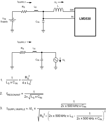 Figure 57. Input RLC Network