SNVSAF9A August 2016 – November 2017 LM5161-Q1
PRODUCTION DATA.
- 1 Features
- 2 Applications
- 3 Description
- 4 Revision History
- 5 Pin Configuration and Functions
- 6 Specifications
-
7 Detailed Description
- 7.1 Overview
- 7.2 Functional Block Diagram
- 7.3
Feature Description
- 7.3.1 Control Circuit
- 7.3.2 VCC Regulator
- 7.3.3 Regulation Comparator
- 7.3.4 Soft-Start
- 7.3.5 Error Transconductance (GM) Amplifier
- 7.3.6 On-Time Generator
- 7.3.7 Current Limit
- 7.3.8 N-Channel Buck Switch and Driver
- 7.3.9 Synchronous Rectifier
- 7.3.10 Enable / Undervoltage Lockout (EN/UVLO)
- 7.3.11 Thermal Protection
- 7.3.12 Ripple Configuration
- 7.4 Device Functional Modes
-
8 Applications and Implementation
- 8.1 Application Information
- 8.2
Typical Applications
- 8.2.1
LM5161-Q1 Synchronous Buck (15-V to 95-V Input, 12-V Output, 1-A Load)
- 8.2.1.1 Design Requirements
- 8.2.1.2
Detailed Design Procedure
- 8.2.1.2.1 Custom Design With WEBENCH® Tools
- 8.2.1.2.2 Output Resistor Divider Selection
- 8.2.1.2.3 Frequency Selection
- 8.2.1.2.4 Inductor Selection
- 8.2.1.2.5 Output Capacitor Selection
- 8.2.1.2.6 Series Ripple Resistor - RESR (FPWM = 1)
- 8.2.1.2.7 VCC and Bootstrap Capacitor
- 8.2.1.2.8 Input Capacitor Selection
- 8.2.1.2.9 Soft-Start Capacitor Selection
- 8.2.1.2.10 EN/UVLO Resistor Selection
- 8.2.1.3 Application Curves
- 8.2.2 LM5161-Q1 Isolated Fly-Buck (36-V to 72-V Input, 12-V, 12-W Isolated Output)
- 8.2.1
LM5161-Q1 Synchronous Buck (15-V to 95-V Input, 12-V Output, 1-A Load)
- 8.3 Do's and Don'ts
- 9 Power Supply Recommendations
- 10Layout
- 11Device and Documentation Support
- 12Mechanical, Packaging, and Orderable Information
Package Options
Mechanical Data (Package|Pins)
- PWP|14
Thermal pad, mechanical data (Package|Pins)
- PWP|14
Orderable Information
8 Applications and Implementation
NOTE
Information in the following applications sections is not part of the TI component specification, and TI does not warrant its accuracy or completeness. TI’s customers are responsible for determining suitability of components for their purposes. Customers should validate and test their design implementation to confirm system functionality.
8.1 Application Information
The LM5161-Q1 is a synchronous-buck regulator converter designed to operate over a wide input voltage and output current range. Spreadsheet based Quick-Start Calculator tools, available on the www.ti.com product website, can be used to design a single output synchronous buck converter or an isolated dual output Fly-Buck converter using the LM5161-Q1. See application note Designing an Isolated Buck (Fly-Buck) Converter for a detailed design guide for the Fly-Buck converter. Alternatively, the online WEBENCH® Tool can be used to create a complete buck or Fly-Buck designs and generate the bill of materials, estimated efficiency, solution size, and cost of the complete solution.Typical Applications describes a few application circuits using the LM5161-Q1 with detailed, step-by-step design procedures.
8.2 Typical Applications
8.2.1 LM5161-Q1 Synchronous Buck (15-V to 95-V Input, 12-V Output, 1-A Load)
A typical application example is a synchronous buck converter operating from a wide input voltage range of 15 V to 95 V and providing a stable 12 V output voltage with maximum output current capability of 1 A. The complete schematic for a typical buck application circuit with LM5161-Q1 in diode emulation is shown in Figure 25 . In the application schematic below, the components are labeled by their respective component numbers instead of the descriptive name used in the previous sections. For example, R1 represents RON and so on.
 Figure 25. Synchronous Buck Application Circuit
8.2.1.1 Design Requirements
A typical synchronous-buck application introduced in LM5161-Q1 Synchronous Buck (15-V to 95-V Input, 12-V Output, 1-A Load), Table 4 summarizes the operating parameters:
Table 4. Design Parameters
| DESIGN PARAMETER | EXAMPLE VALUE |
|---|---|
| Input voltage range | 15-V to 80-V |
| output | 12-V |
| Full load current | 1-A |
| Nominal switching frequency | 300 kHz |
| Light load operating mode | CCM, FPWM=1 |
| Jumper JP1 | Pins 1-2 connected |
8.2.1.2 Detailed Design Procedure
8.2.1.2.1 Custom Design With WEBENCH® Tools
Click here to create a custom design using the LM5161-Q1 device with the WEBENCH® Power Designer.
- Start by entering the input voltage (VIN), output voltage (VOUT), and output current (IOUT) requirements.
- Optimize the design for key parameters such as efficiency, footprint, and cost using the optimizer dial.
- Compare the generated design with other possible solutions from Texas Instruments.
The WEBENCH Power Designer provides a customized schematic along with a list of materials with real-time pricing and component availability.
In most cases, these actions are available:
- Run electrical simulations to see important waveforms and circuit performance
- Run thermal simulations to understand board thermal performance
- Export customized schematic and layout into popular CAD formats
- Print PDF reports for the design, and share the design with colleagues
Get more information about WEBENCH tools at www.ti.com/WEBENCH.
8.2.1.2.2 Output Resistor Divider Selection
With the required output voltage set point at 12 V and VFB = 2 V (typical), the ratio of R8 (RFB1) to R7 (RFB2) can be calculated using Equation 9:

The resistor ratio calculates to be 5:1. Standard values of R8 (RFB1) = 2 kΩ and R7 (RFB2 ) =10 kΩ are chosen. Higher or lower resistor values could be used as long as the ratio of 5:1 is maintained.
8.2.1.2.3 Frequency Selection
The duty cycle required to maintain output regulation at the minimum input voltage restricts the maximum switching frequency of LM5161-Q1. The maximum value of the minimum forced OFF-time TOFF,min (max), limits the duty cycle and therefore the switching frequency. The maximum frequency that avoids output dropout at minimum input voltage can be calculated from Equation 10.

For this design example, the maximum frequency based on the minimum OFF-time limitation for TOFF,min(typical) = 170 ns is calculated to be FSW,max(@VIN,min) = 1.2 MHz. This value is above 1 MHz, the maximum possible operating frequency of the LM5161-Q1. Therefore, the minimum OFF-time parameter restricts the maximum achievable switching frequency calculation in this application.
At the maximum input voltage, the maximum switching frequency of LM5161-Q1 is restricted by the minimum ON-time, TON,min which limits the minimum duty cycle of the converter. The maximum frequency at maximum input voltage can be calculated using Equation 11.

Using Equation 11 and TON,min (typ) = 150 ns, the maximum achievable switching frequency is FSW,max(@VIN,min)= 1000 kHz. Taking this value as the maximum possible operational switching frequency over the input voltage range in this application, a nominal switching frequency of FSW = 300 kHz is chosen for this design.
The value of the resistor, RON sets the nominal switching frequency based on Equation 12.

For this particular application with FSW = 300 kHz, RON calculates to be 396 kΩ . Selecting a standard value for R1 (RON) = 402 kΩ (±1%) results in a nominal frequency of 296 kHz. The resistor value may need to adjusted further in order to achieve the required switching frequency as the switching frequency in Constant ON-Time converters varies slightly(±10%) with input voltage and/or output current. Operation at a lower nominal switching frequency will result in higher efficiency but increase in the inductor and capacitor values leading to a larger total solution size.
8.2.1.2.4 Inductor Selection
The inductor is selected to limit the inductor ripple current to a value between 20 and 40 percent of the maximum load current. The minimum value of the inductor required in this application can be calculated from Equation 13:

Based on Equation 13 , the minimum value of the inductor is calculated to be 85 µH for VIN = 80-V (max) and inductor current ripple will be 40 percent of the maximum load current. Allowing some margin for inductance variation and inductor saturation, a higher standard value of L1 (L) = 100 µH is selected for this design.
The peak inductor current at maximum load must be smaller than the minimum current limit threshold of the high side FET as given in Electrical Characteristics table. The inductor current ripple at any input voltage is given by:

The peak-to-peak inductor current ripple is calculated to be 81 mA and 341 mA at the minimum and maximum input voltages respectively. The maximum peak inductor current in the buck FET is given by Equation 15:

In this design with maximum output current of 1-A, the maximum peak inductor current is calculated to be approximately 1.17 A at VIN,max = 80 V, which is less than the minimum high-side FET current limit threshold.
The saturation current of the inductor must also be carefully considered. The peak value of the inductor current will be bound by the high side FET current limit during overload or short circuit conditions. Based on the high side FET current limit specification in the Electrical Characteristics, an inductor with saturation current rating above 1.9 A (max) should be selected.
8.2.1.2.5 Output Capacitor Selection
The output capacitor is selected to limit the capacitive ripple at the output of the regulator. Maximum capacitive ripple is observed at maximum input voltage. The output capacitance required for a ripple voltage ∆VO across the capacitor is given by Equation 16.

Substituting ∆VO, ripple = 10 mV gives COUT = 15 μF. Two standard 10 μF ceramic capacitors in parallel (C11, C12) are selected. An X7R type capacitor with a voltage rating 25 V or higher should be used for COUT (C11, C12) to limit the reduction of capacitance due to dc bias voltage.
8.2.1.2.6 Series Ripple Resistor - RESR (FPWM = 1)
If the FPWM = 1, i.e. the FPWM pin is pulled high as when connected to VCC, a series resistor in series with the output capacitor or the external ripple injection circuit must be selected such that sufficient ripple injection (> 25mV) is ensured at the feedback pin FB. The ripple produced by RESR is proportional to the inductor current ripple, and therefore, RESR should be chosen for minimum inductor current ripple which occurs at minimum input voltage. The RESR is calculated by Equation 17.

With VO = 12 V, VREF = 2 V and ΔIL, min = 81 mA (at VIN, min= 15 V) as calculated in Equation 14, Equation 17 requires an RESR greater than or equal to 1.87 Ω. Selecting R4 (RESR) = 2 Ω results in approximately 700 mV of maximum output voltage ripple at VIN,max. However due to the internal DC Error correction loop, the load and line regulation will be much improved, despite the addition of a large RESR in the circuit. For applications which require even lower output voltage ripple, Type 2 or Type 3 ripple injection circuits must be used, as described in Ripple Configuration. In this design example, with the FPWM =1 (i.e. the FPWM pin is pulled up to VCC) a 0 Ω ESR resistor is selected and the external Type 3 ripple injection circuit is used.
8.2.1.2.7 VCC and Bootstrap Capacitor
The VCC capacitor charges the bootstrap capacitor during the OFF-time of the high-side switch and powers internal logic circuits and the low side sync FET gate driver. The bootstrap capacitor biases the high-side gate driver during the high-side FET ON-time. A good value for C13 (CVCC) is 1 µF. A good choice for C1 (CBST) is 10 nF. Both must be high quality X7R ceramic capacitors.
8.2.1.2.8 Input Capacitor Selection
The input capacitor must be large enough to limit the input voltage ripple to an acceptable level. Equation 18 provides the input capacitance CIN required for a worst case input ripple of ∆VIN, ripple.
CIN (C4, C6) supplies most of the switch current during the ON-time to limit the voltage ripple at the VIN pin. At maximum load current, when the buck switch turns on, the current into the VIN pin quickly increases to the valley current of the inductor ripple and then ramps up to the peak of the inductor ripple during the ON-time of the high-side FET. The average current during the ON-time is the output load current. For a worst-case calculation, CIN must supply this average load current during the maximum ON-time, without letting the voltage at VIN drop more than the desired input ripple. For this design, the input voltage drop is limited to 0.5 V and the value of CIN is calculated using Equation 18.
Based on Equation 18, the value of the input capacitor is calculated to be approximately 1.68 µF at D = 0.5. Taking into account the decrease in capacitance over an applied voltage, two standard value ceramic capacitors of 2.2 μF are selected for C4 and C6. The input capacitors should be rated for the maximum input voltage under all operating and transient conditions. A 100-V, X7R dielectric was selected for this design.
A third input capacitor C5 is needed in this design as a bypass path for the high frequency component of the input switching current. The value of C5 is 0.1 μF and this bypass capacitor must be placed directly across VIN and PGND (pin 3 and 2) near the IC. The CIN values and location are critical to reducing switching noise and transients.
8.2.1.2.9 Soft-Start Capacitor Selection
The capacitor at the SS pin determines the soft-start time, that is the time for the output voltage to reach its final steady state value. The capacitor value is determined from Equation 19:

With C9 (CSS) set at 22 nF and the Vss = 2 V, ISS = 10 µA, the TStartup should measure approximately 4 ms.
8.2.1.2.10 EN/UVLO Resistor Selection
The UVLO resistors R3 (RUV2) and R9 (RUV1) set the input undervoltage lockout threshold and hysteresis according to Equation 20 and Equation 21:

and,

From the Electrical Characteristics, IUVLO(HYS) = 20 μA (typical). To design for VIN rising threshold (VIN, UVLO(rising)) at 15 V and EN/UVLO hysteresis of 1.5 V, Equation 20 and Equation 21 yield RUV1 = 6.81 kΩ and RUV2 = 75 kΩ . Selecting 1% standard value of R9 (RUV1) = 6.81 kΩ and R3 (RUV2) = 75 kΩ results in UVLO threshold (rising) and hysteresis of 14.9 V and 1.5 V respectively.
8.2.1.3 Application Curves
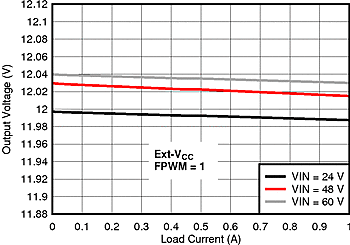 Figure 26. Load Regulation
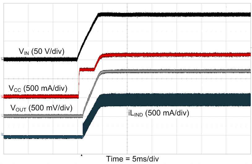 Figure 28. EN/UVLO Startup at VIN= 48 V and IOUT = 1 A
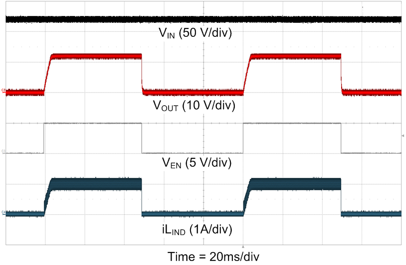 Figure 30. EN/UVLO Startup at VIN= 48 V and RLOAD = 12 Ω at FPWM = 1
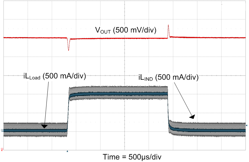 Figure 32. Load Transient (0 A - 1 A) at VIN = 48 V
at FPWM = 1
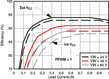 Figure 27. Efficiency vs IOUT (FPWM = 1)
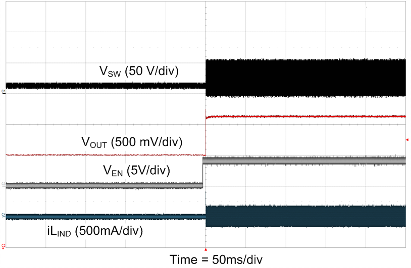 Figure 29. Pre-Bias (11.5 V) Startup at VIN= 48 V at No Load & FPWM = 1
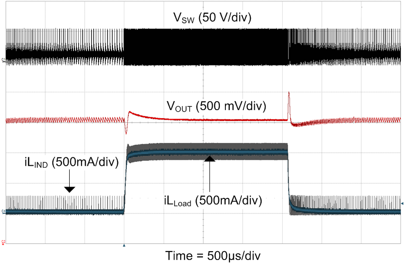 Figure 31. Load Transient (0 A - 1 A) at VIN = 48 V
at FPWM = 0
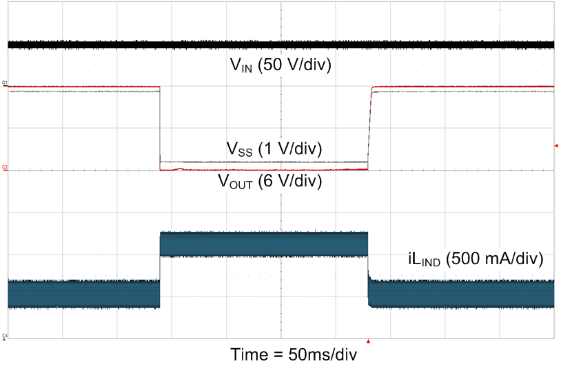 Figure 33. Output Short-Circuit at VIN = 48 V
 (Full Load to Short)
8.2.2 LM5161-Q1 Isolated Fly-Buck (36-V to 72-V Input, 12-V, 12-W Isolated Output)
A typical application example for an isolated Fly-Buck converter operates over an input voltage range of 36 V to 72 V. It provides a stable 12 V isolated output voltage with output power capability of 10 W. The complete schematic of the Fly-Buck application circuit is shown in Figure 34.
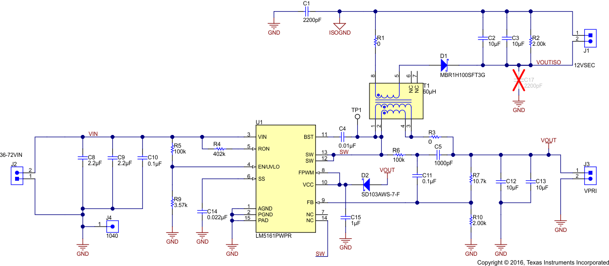 Figure 34. 12-V, 10-W Fly-Buck Schematic
8.2.2.1 LM5161-Q1 Fly-Buck Design Requirements
The LM5161-Q1 Fly-Buck application example is designed to operate from a nominal 48-V DC supply with line variations from 36-V to 72-V. This example provides a space-optimized and efficient 12-V isolated output solution with secondary load current capability from 0-A to 800 mA. The primary side remains unloaded in this application. The switching frequency is set at 300 kHz (nominal). This design achieves greater than 88% peak efficiency.
Table 5. Design Parameters
| DESIGN PARAMETER | EXAMPLE VALUE |
|---|---|
| Input voltage range | 36 V - 72 V |
| Isolated output | 12 V (+/- 10%) |
| Isolated load current range (IISO) | 0-A to 0.8-A |
| Nominal switching frequency | 300 KHz |
| Peak efficiency | ~87% |
| Operation mode | FPWM = 1 |
8.2.2.2 Detailed Design Procedure
The Fly-Buck converter design procedure closely follows the buck converter design outlined in LM5161-Q1 Synchronous Buck (15-V to 95-V Input, 12-V Output, 1-A Load). The selection of primary output voltage, transformer turns ratio, rectifier diode, and output capacitors are covered here.
8.2.2.2.1 Selection of VOUT and Turns Ratio
The primary output voltage in a Fly-Buck converter should be no more than one half of the minimum input voltage. Therefore, at the minimum VIN of 36 V, the primary output voltage ( VOUT ) should be no higher than 18 V. The isolated output voltage of VOUTISO in Figure 34 is set at 12 V by selecting a transformer with a turns ratio (N1:N2 :: NPRI:NSEC) of 1:1. Using this turns ratio, the required primary output voltage VOUT is calculated in Equation 22:

The 0.7 V (VFD1) added to VOUTISO in Equation 22 represents the forward voltage drop of the secondary rectifier diode. By setting the primary output voltage VOUT to 12.7-V by selecting the correct feedback resistors, the secondary voltage is regulated at 12-V nominally. Adjustment of the primary side VOUT may be required to compensate for voltage errors due to the leakage inductance of the transformer, the resistance of the transformer windings, the diode drop in the power path on the secondary side and the low-side FET of the LM5161-Q1.
8.2.2.2.2 Secondary Rectifier Diode
The secondary side rectifier diode must block the maximum input voltage reflected at secondary side switch node. The minimum diode reverse voltage V(RD1) rating is given in Equation 23:

A diode of 100-V or higher reverse voltage rating must be selected in this application. If the input voltage (VIN) has transients above the normal operating maximum input voltage of 72 V, then the worst-case transient input voltage must be used in the Equation 23 while selecting the secondary side rectifier diode.
8.2.2.2.3 External Ripple Circuit
The FPWM pin in the LM5161-Q1 should never be grounded or left open when used in a Fly-Buck application. Type 3 ripple circuit is required for Fly-Buck applications. Follow the design procedure used in the buck converter for selecting the Type 3 ripple injection components. See Ripple Configuration for ripple design information.
8.2.2.2.4 Output Capacitor (CVISO)
The Fly-Buck output capacitor conducts higher ripple current than a buck converter output capacitor. The ripple voltage across the isolated output capacitor is calculated based on the time the rectifier diode is off. During this time the entire output current is supplied by the output capacitor. The required capacitance for the worst-case ripple voltage can be calculated using Equation 24 where, ΔVISO is the expected ripple voltage at the secondary output.

Equation 24 is an approximation and ignores the ripple components associated with ESR and ESL of the output capacitor. For a ΔVISO = 100 mV, Equation 24 requires CVISO = 11.12 µF. When selecting the CVISO output capacitors (C2 and C3 in the Figure 34), the DC bias must be considered in order to ensure sufficient capacitance over the output voltage.
8.2.2.3 Application Curves
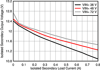 Figure 35. Load Regulation
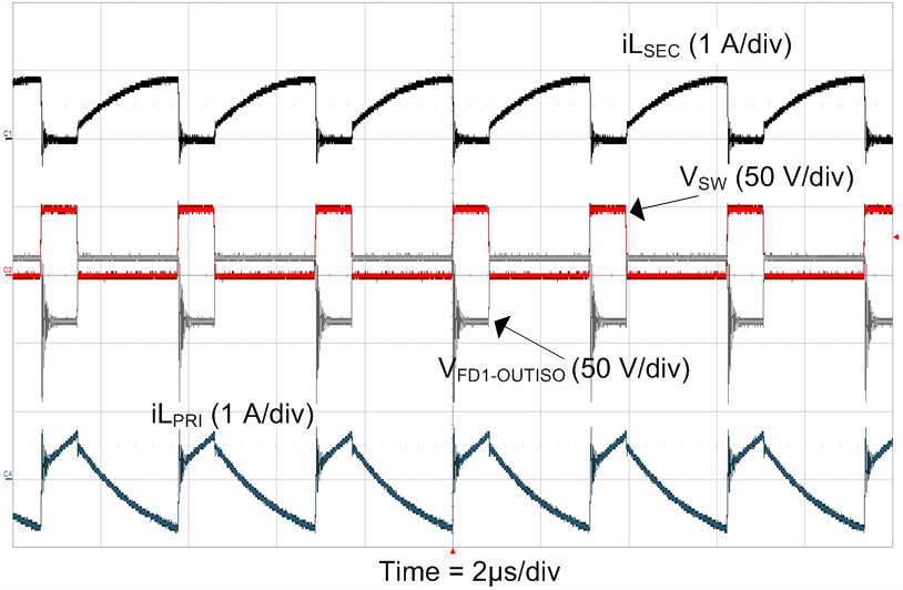 Figure 37. Steady State at VIN = 48 V
 and IOUT2 = 500 mA
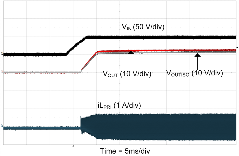 Figure 39. VIN Startup at IISO = 500 mA
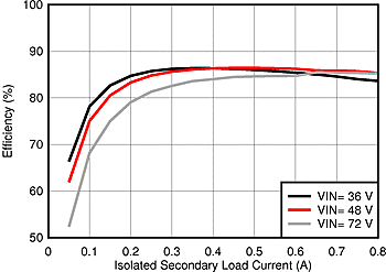 Figure 36. Efficiency vs. IISO
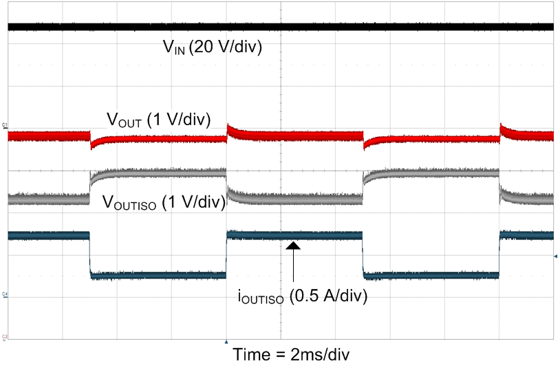 Figure 38. Secondary Load Transient
 at IISO = 250 mA - 750 mA
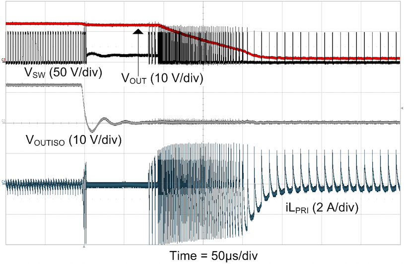 Figure 40. Secondary-Side Short at IOUT2 = 0 A
 and IPRI = 0 A
8.3 Do's and Don'ts
As mentioned earlier in Soft-Start, the SS capacitor CSS, must be more than 1 nF in both Buck and Fly-Buck applications. Apart from determining the startup time, this capacitor serves for the external compensation of the internal GM error amplifier. A minimum value of 1 nF is necessary to maintain stability. The SS pin must not be left floating.
When the FPWM pin is shorted to ground or left unconnected, no external ripple injection is necessary in a Buck application. Should an external feedback ripple circuit be configured when FPWM = 0, it will produce higher ripple at the output.
Add a resistor (>3Ω) in series with the BST capacitor when using the part in FPWM = 0, as described in detail in Forced Pulse Width Modulation (FPWM) Mode.
When configured as a Fly-Buck, the FPWM pin should always be connected to VCC. A Fly-Buck application must operate in the continuous conduction mode all the time in order to maintain adequate voltage regulation on the secondary side. FPWM = 0 is not a valid mode in the Fly-Buck application.
