SNVSAF9A August 2016 – November 2017 LM5161-Q1
PRODUCTION DATA.
- 1 Features
- 2 Applications
- 3 Description
- 4 Revision History
- 5 Pin Configuration and Functions
- 6 Specifications
-
7 Detailed Description
- 7.1 Overview
- 7.2 Functional Block Diagram
- 7.3
Feature Description
- 7.3.1 Control Circuit
- 7.3.2 VCC Regulator
- 7.3.3 Regulation Comparator
- 7.3.4 Soft-Start
- 7.3.5 Error Transconductance (GM) Amplifier
- 7.3.6 On-Time Generator
- 7.3.7 Current Limit
- 7.3.8 N-Channel Buck Switch and Driver
- 7.3.9 Synchronous Rectifier
- 7.3.10 Enable / Undervoltage Lockout (EN/UVLO)
- 7.3.11 Thermal Protection
- 7.3.12 Ripple Configuration
- 7.4 Device Functional Modes
-
8 Applications and Implementation
- 8.1 Application Information
- 8.2
Typical Applications
- 8.2.1
LM5161-Q1 Synchronous Buck (15-V to 95-V Input, 12-V Output, 1-A Load)
- 8.2.1.1 Design Requirements
- 8.2.1.2
Detailed Design Procedure
- 8.2.1.2.1 Custom Design With WEBENCH® Tools
- 8.2.1.2.2 Output Resistor Divider Selection
- 8.2.1.2.3 Frequency Selection
- 8.2.1.2.4 Inductor Selection
- 8.2.1.2.5 Output Capacitor Selection
- 8.2.1.2.6 Series Ripple Resistor - RESR (FPWM = 1)
- 8.2.1.2.7 VCC and Bootstrap Capacitor
- 8.2.1.2.8 Input Capacitor Selection
- 8.2.1.2.9 Soft-Start Capacitor Selection
- 8.2.1.2.10 EN/UVLO Resistor Selection
- 8.2.1.3 Application Curves
- 8.2.2 LM5161-Q1 Isolated Fly-Buck (36-V to 72-V Input, 12-V, 12-W Isolated Output)
- 8.2.1
LM5161-Q1 Synchronous Buck (15-V to 95-V Input, 12-V Output, 1-A Load)
- 8.3 Do's and Don'ts
- 9 Power Supply Recommendations
- 10Layout
- 11Device and Documentation Support
- 12Mechanical, Packaging, and Orderable Information
Package Options
Mechanical Data (Package|Pins)
- PWP|14
Thermal pad, mechanical data (Package|Pins)
- PWP|14
Orderable Information
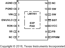
5 Pin Configuration and Functions
PWP Package
14-Pin HTSSOP
TOP

Pin Functions
| PIN | I/O | DESCRIPTION | |
|---|---|---|---|
| NAME | HTSSOP | ||
| AGND | 1 | - | Analog Ground. Ground connection of internal control circuits. |
| PGND | 2 | - | Power Ground. Ground connection of the internal synchronous rectifier FET. |
| VIN | 3 | I | Input supply connection. Operating input range is 4.5-V to 100-V. |
| EN/UVLO | 4 | I | Precision enable. Input pin of undervoltage lockout (UVLO) comparator. |
| RON | 5 | I | On-time programming pin. A resistor between this pin and VIN sets the switch ON-time as a function of input voltage. |
| SS | 6 | I | Softstart. Connect a capacitor from SS to AGND to control output rise time and limit overshoot. |
| FPWM | 8 | I | Forced PWM logic input pin. Connect to AGND for discontinuous conduction mode (DCM) with light loads. Connect to VCC for continuous conduction mode (CCM) at all loads and Fly-Buck configuration. |
| FB | 9 | I | Feedback input of voltage regulation comparator. |
| VCC | 10 | O | Internal high voltage start-up regulator bypass capacitor pin. |
| BST | 11 | I | Bootstrap capacitor pin. Connect a capacitor between BST and SW to bias gate driver of high-side buck FET. |
| SW | 12,13 | O | Switch node. Source connection of high side buck FET and drain connection of low-side synchronous rectifier FET. |
| NC | 7,14 | No Connection. | |
| EP | - | Exposed Pad. Connect to AGND and printed-circuit board ground plane to improve power dissipation. | |