SNOS750A August 1999 – October 2014 LM7121
PRODUCTION DATA.
- 1Features
- 2Applications
- 3Description
- 4Revision History
- 5Pin Configuration and Functions
-
6Specifications
- 6.1 Absolute Maximum Ratings
- 6.2 Handling Ratings
- 6.3 Recommended Operating Conditions
- 6.4 Thermal Information
- 6.5 ±15V DC Electrical Characteristics
- 6.6 ±15V AC Electrical Characteristics
- 6.7 ±5V DC Electrical Characteristics
- 6.8 ±5V AC Electrical Characteristics
- 6.9 +5V DC Electrical Characteristics
- 6.10 +5V AC Electrical Characteristics
- 6.11 Typical Characteristics
- 7Application and Implementation
- 8Device and Documentation Support
- 9Mechanical, Packaging, and Orderable Information
Package Options
Refer to the PDF data sheet for device specific package drawings
Mechanical Data (Package|Pins)
- D|8
- DBV|5
Thermal pad, mechanical data (Package|Pins)
Orderable Information
6 Specifications
6.1 Absolute Maximum Ratings(1)
over operating free-air temperature range (unless otherwise noted) (1)| MIN | MAX | UNIT | ||
|---|---|---|---|---|
| Differential Input Voltage (2) | ±2 | V | ||
| Voltage at Input/Output Pins | (V+)−1.4, (V−)+1.4 |
V | ||
| Supply Voltage (V+–V−) | 36 | V | ||
| Output Short Circuit to Ground (3) | Continuous | |||
| Lead Temperature (soldering, 10 sec) | 260 | °C | ||
| Junction Temperature(4) | 150 | ˚C | ||
(1) Stresses beyond those listed under Absolute Maximum Ratings may cause permanent damage to the device. These are stress ratings only, which do not imply functional operation of the device at these or any other conditions beyond those indicated under Recommended Operating Conditions. Exposure to absolute-maximum-rated conditions for extended periods may affect device reliability.
(2) Applies to both single-supply and split-supply operation. Continuous short circuit operation at elevated ambient temperature can result in exceeding the maximum allowed junction temperature of 150°C.
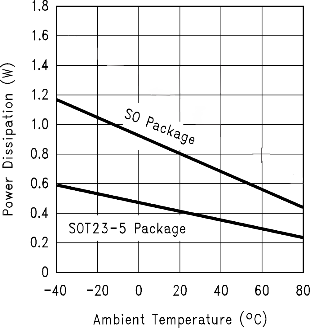
(3) The maximum power dissipation is a function of TJ(max), RθJA, and TA. The maximum allowable power dissipation at any ambient temperature is PD = (TJ(max)–TA)/RθJA. All numbers apply for packages soldered directly into a PC board.
(4) Typical Values represent the most likely parametric norm.
(5) All limits are ensured by testing or statistical analysis.
(6) Slew rate is the average of the rising and falling slew rates.
(7) Unity gain operation for ±5 V and ±15 V supplies is with a feedback network of 510 Ω and 3 pF in parallel (see Application and Implementation). For +5V single supply operation, feedback is a direct short from the output to the inverting input.
(8) AV = +2 operation with 2 kΩ resistors and 2 pF capacitor from summing node to ground.
6.2 Handling Ratings
| MIN | MAX | UNIT | |||
|---|---|---|---|---|---|
| Tstg | Storage temperature range | −65 | +150 | °C | |
| V(ESD) | Electrostatic discharge | Human body model (HBM), per ANSI/ESDA/JEDEC JS-001, all pins(1) | 2000 | V | |
(1) JEDEC document JEP155 states that 2000-V HBM allows safe manufacturing with a standard ESD control process. Human body model, 1.5 k in series with 100 pF.
6.3 Recommended Operating Conditions
over operating free-air temperature range (unless otherwise noted)| MIN | NOM | MAX | UNIT | ||
|---|---|---|---|---|---|
| Operating Temperature Range | -40 | 85 | °C | ||
6.4 Thermal Information
| THERMAL METRIC(1) | D0008A (8) | DBV (5) | UNIT | |
|---|---|---|---|---|
| RθJA | Junction-to-ambient thermal resistance | 165 | 325 | °C/W |
(1) For more information about traditional and new thermal metrics, see the IC Package Thermal Metrics application report, SPRA953.
6.5 ±15V DC Electrical Characteristics
Unless otherwise specified, all limits ensured for V+ = +15V, V− = −15V, VCM = VO = 0 V and RL > 1 MΩ. Boldface limits apply at the temperature extremes.| PARAMETER | TEST CONDITIONS | TYP(4) | LM7121I LIMIT(5) |
UNIT | |
|---|---|---|---|---|---|
| VOS | Input Offset Voltage | 0.9 | 8 15 |
mV max |
|
| IB | Input Bias Current | 5.2 | 9.5 12 |
µA max |
|
| IOS | Input Offset Current | 0.04 | 4.3 7 |
µA max |
|
| RIN | Input Resistance | Common Mode | 10 | MΩ | |
| Differential Mode | 3.4 | MΩ | |||
| CIN | Input Capacitance | Common Mode | 2.3 | pF | |
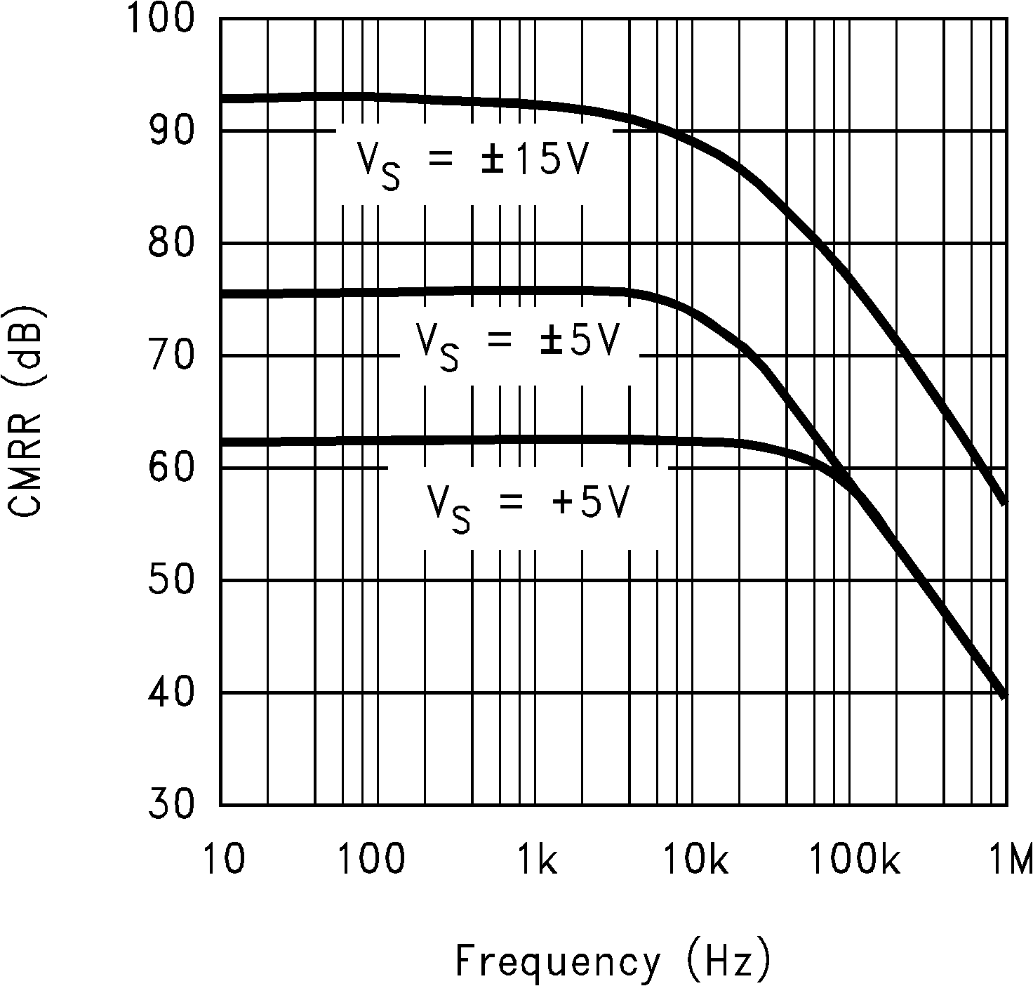
| CMRR | Common Mode Rejection Ratio | −10V ≤ VCM ≤ 10V |
93 |
73 70 |
dB min |
| +PSRR | Positive Power Supply Rejection Ratio | 10V ≤ V+ ≤ 15 V | 86 |
70 68 |
dB min |
| −PSRR | Negative Power Supply Rejection Ratio | −15V ≤ V− ≤ −10V | 81 |
68 65 |
dB min |
| VCM | Input Common-Mode Voltage Range | CMRR ≥ 70 dB | 13 | 11 | V min |
| −13 | −11 | V max | |||
| AV | Large Signal Voltage Gain | RL = 2 kΩ , VO = 20 VPP | 72 |
65 57 |
dB min |
| VO | Output Swing | RL = 2 kΩ | 13.4 |
11.1 10.8 |
V min |
| −13.4 |
−11.2 −11.0 |
V max |
|||
| RL = 150 Ω | 10.2 |
7.75 7.0 |
V min |
||
| −7.0 |
−5.0 −4.8 |
V max |
|||
| ISC | Output Short Circuit Current | Sourcing | 71 |
54 44 |
mA min |
| Sinking | 52 |
39 34 |
mA min |
||
| IS | Supply Current | 5.3 |
6.6 7.5 |
mA max |
6.6 ±15V AC Electrical Characteristics
Unless otherwise specified, all limits ensured for V+ = 15V, V− = −15V, VCM = VO = 0 V and RL > 1 MΩ. Boldface limits apply at the temperature extremes.| PARAMETER | TEST CONDITIONS | TYP(4) | LM7121I LIMIT(5) |
UNIT | |
|---|---|---|---|---|---|
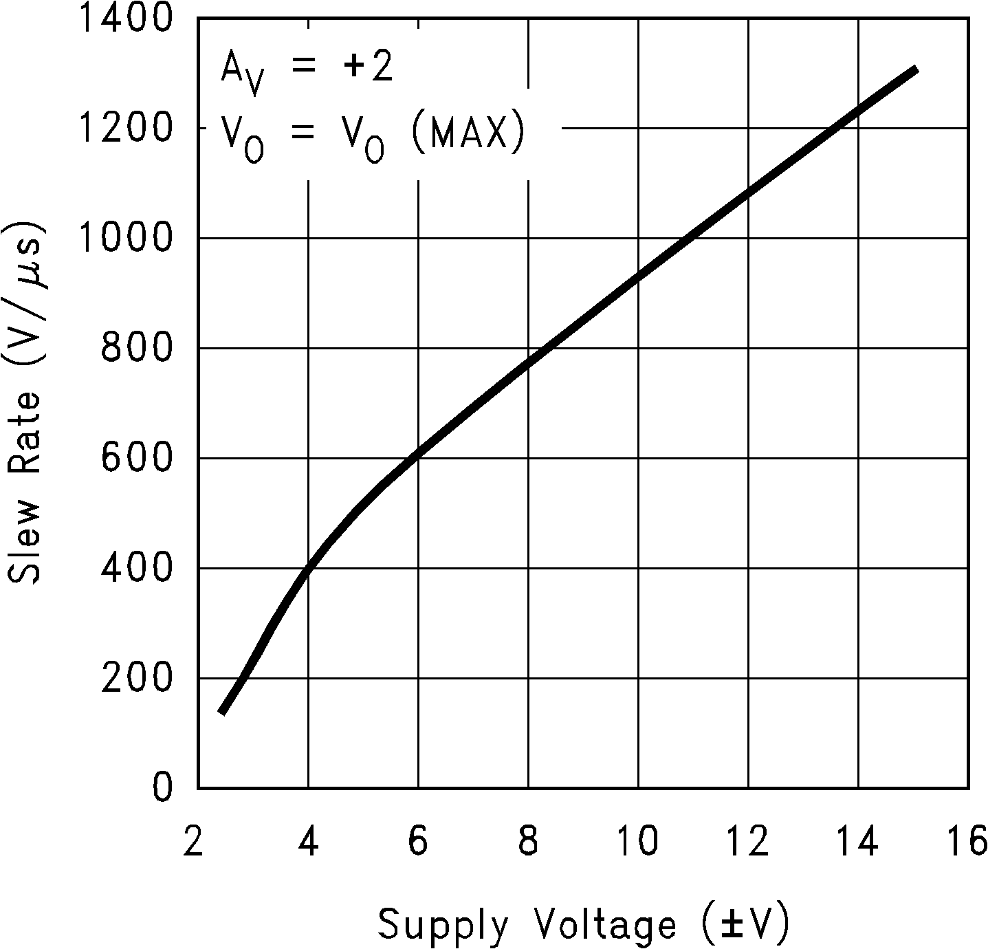
| SR | Slew Rate(6) | AV = +2, RL = 1 kΩ, VO = 20 VPP | 1300 | V/µs | |
| GBW | Unity Gain-Bandwidth | RL = 1 kΩ | 175 | MHz | |
| Øm | Phase Margin | 63 | Deg | ||
| f (−3 dB) | Bandwidth(7)(8) | RL = 100 Ω, AV = +1 | 235 | MHz | |
| RL = 100 Ω, AV = +2 | 50 | ||||
| ts | Settling Time | 10 VPP Step, to 0.1%, RL = 500 Ω | 74 | ns | |
| tr, tf | Rise and Fall Time(8) | AV = +2, RL = 100 Ω, VO = 0.4 VPP | 5.3 | ns | |
| AD | Differential Gain | AV = +2, RL = 150 Ω | 0.3% | ||
| ØD | Differential Phase | AV = +2, RL = 150 Ω | 0.65 | Deg | |
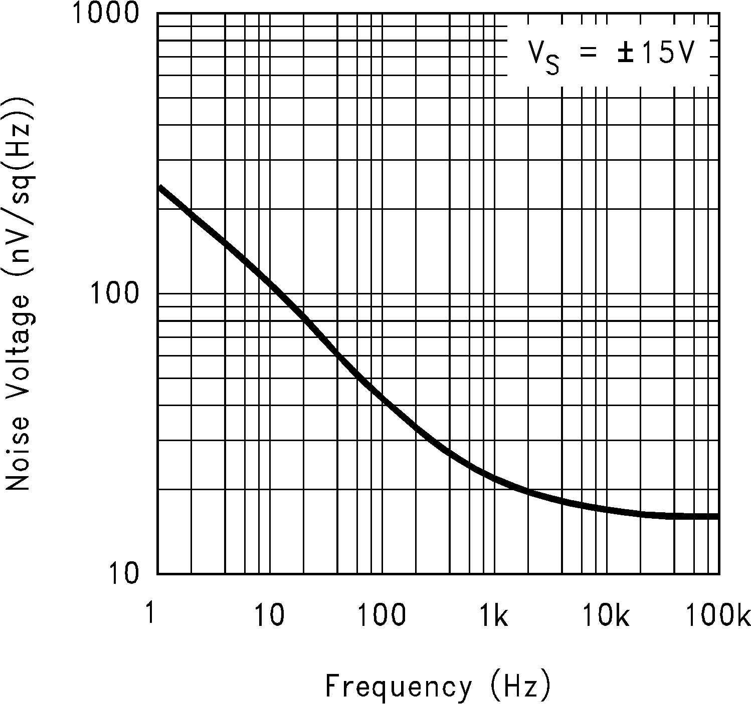
| en | Input-Referred Voltage Noise | f = 10 kHz | 17 | nV / √HZ | |
| in | Input-Referred Current Noise | f = 10 kHz | 1.9 | pA / √HZ | |
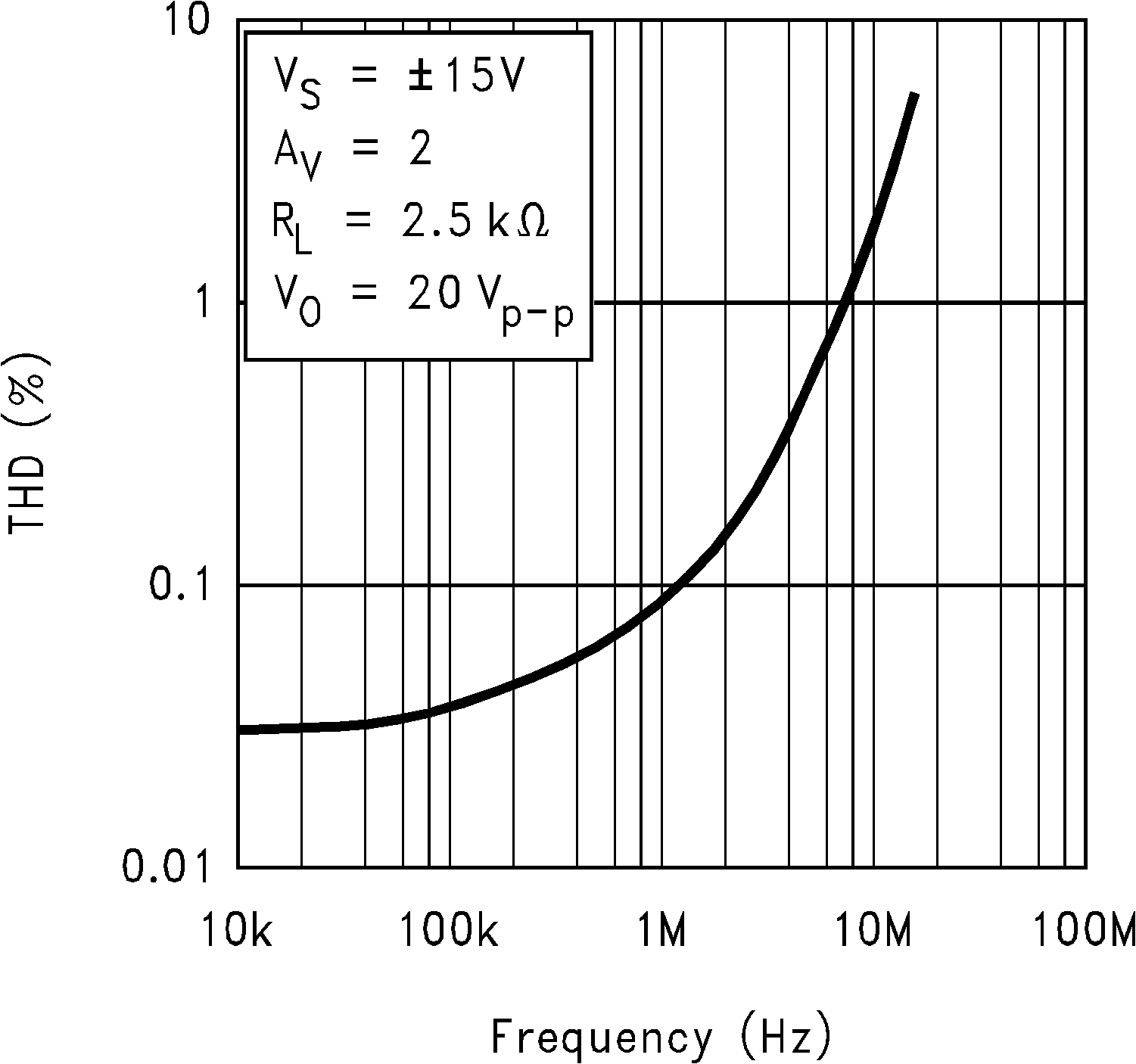
| T.H.D. | Total Harmonic Distortion | 2 VPP Output, RL = 150 Ω, AV = +2, f = 1 MHz |
0.065% | ||
| 2 VPP Output, RL = 150 Ω, AV = +2, f = 5 MHz |
0.52% |
6.7 ±5V DC Electrical Characteristics
Unless otherwise specified, all limits ensured for V+ = 5V, V− = −5V, VCM = VO = 0 V and RL > 1 MΩ. Boldface limits apply at the temperature extremes.| PARAMETER | TEST CONDITIONS | TYP(4) | LM7121I LIMIT(5) |
UNIT | |
|---|---|---|---|---|---|
| VOS | Input Offset Voltage | 1.6 |
8 15 |
mV max |
|
| IB | Input Bias Current | 5.5 |
9.5 12 |
µA max |
|
| IOS | Input Offset Current | 0.07 |
4.3 7.0 |
µA max |
|
| RIN | Input Resistance | Common Mode | 6.8 | MΩ | |
| Differential Mode | 3.4 | MΩ | |||
| CIN | Input Capacitance | Common Mode | 2.3 | pF | |
| CMRR | Common Mode Rejection Ratio | −2V ≤ VCM ≤ 2V | 75 |
65 60 |
dB min |
| +PSRR | Positive Power Supply Rejection Ratio | 3V ≤ V+ ≤ 5V | 89 |
65 60 |
dB min |
| −PSRR | Negative Power Supply Rejection Ratio | −5V ≤ V− ≤ −3V | 78 |
65 60 |
dB min |
| VCM | Input Common Mode Voltage Range | CMRR ≥ 60 dB | 3 |
2.5 |
V min |
| −3 |
−2.5 |
V max |
|||
| AV | Large Signal Voltage Gain | RL = 2 kΩ, VO = 3 VPP | 66 |
60 58 |
dB min |
| VO | Output Swing | RL = 2 kΩ | 3.62 |
3.0 2.75 |
V min |
| −3.62 |
−3.0 −2.70 |
V max |
|||
| RL = 150 Ω | 3.1 |
2.5 2.3 |
V min |
||
| −2.8 |
−2.15 −2.00 |
V max |
|||
| ISC | Output Short Circuit Current | Sourcing | 53 |
38 33 |
mA min |
| Sinking | 29 |
21 19 |
mA min |
||
| IS | Supply Current | 5.1 |
6.4 7.2 |
mA max |
6.8 ±5V AC Electrical Characteristics
Unless otherwise specified, all limits ensured for V+ = 5V, V− = −5V, VCM = VO = 0 V and RL > 1 MΩ. Boldface limits apply at the temperature extremes.| PARAMETER | TEST CONDITIONS | TYP(4) | LM7121I LIMIT(5) |
UNIT | |
|---|---|---|---|---|---|
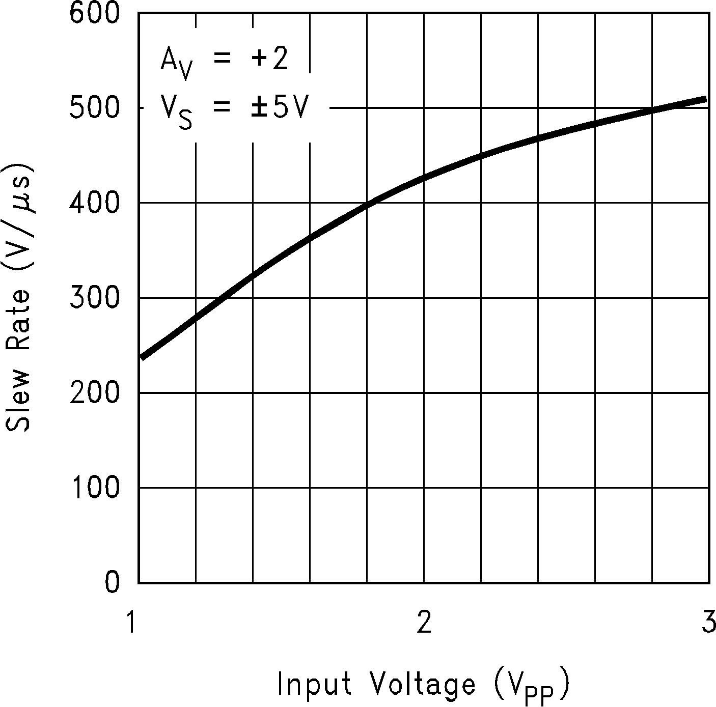
| SR | Slew Rate(6) | AV = +2, RL = 1 kΩ, VO = 6 VPP | 520 | V/µs | |
| GBW | Unity Gain-Bandwidth | RL = 1 kΩ | 105 | MHz | |
| Øm | Phase Margin | RL = 1 kΩ | 74 | Deg | |
| f (−3 dB) | Bandwidth(7)(8) | RL = 100 Ω, AV = +1 | 160 | MHz | |
| RL = 100 Ω, AV = +2 | 50 | MHz | |||
| ts | Settling Time | 5 VPP Step, to 0.1%, RL = 500 Ω | 65 | ns | |
| tr, tf | Rise and Fall Time(8) | AV = +2, RL = 100 Ω, VO = 0.4 VPP | 5.8 | ns | |
| AD | Differential Gain | AV = +2, RL = 150 Ω | 0.3% | ||
| ØD | Differential Phase | AV = +2, RL = 150 Ω | 0.65 | Deg | |
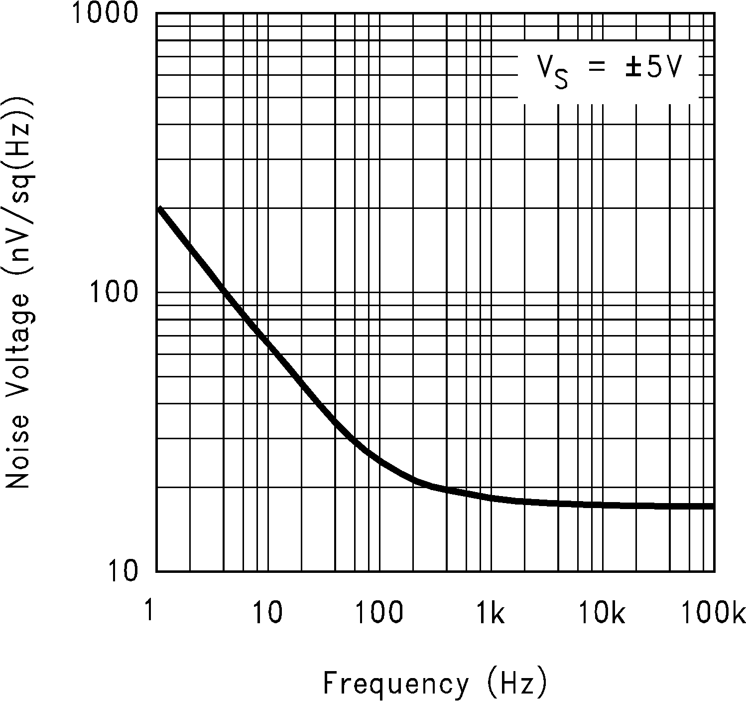
| en | Input-Referred Voltage Noise | f = 10 kHz | 17 | nV / √Hz | |
| in | Input-Referred Current Noise | f = 10 kHz | 2 | pA / √Hz | |
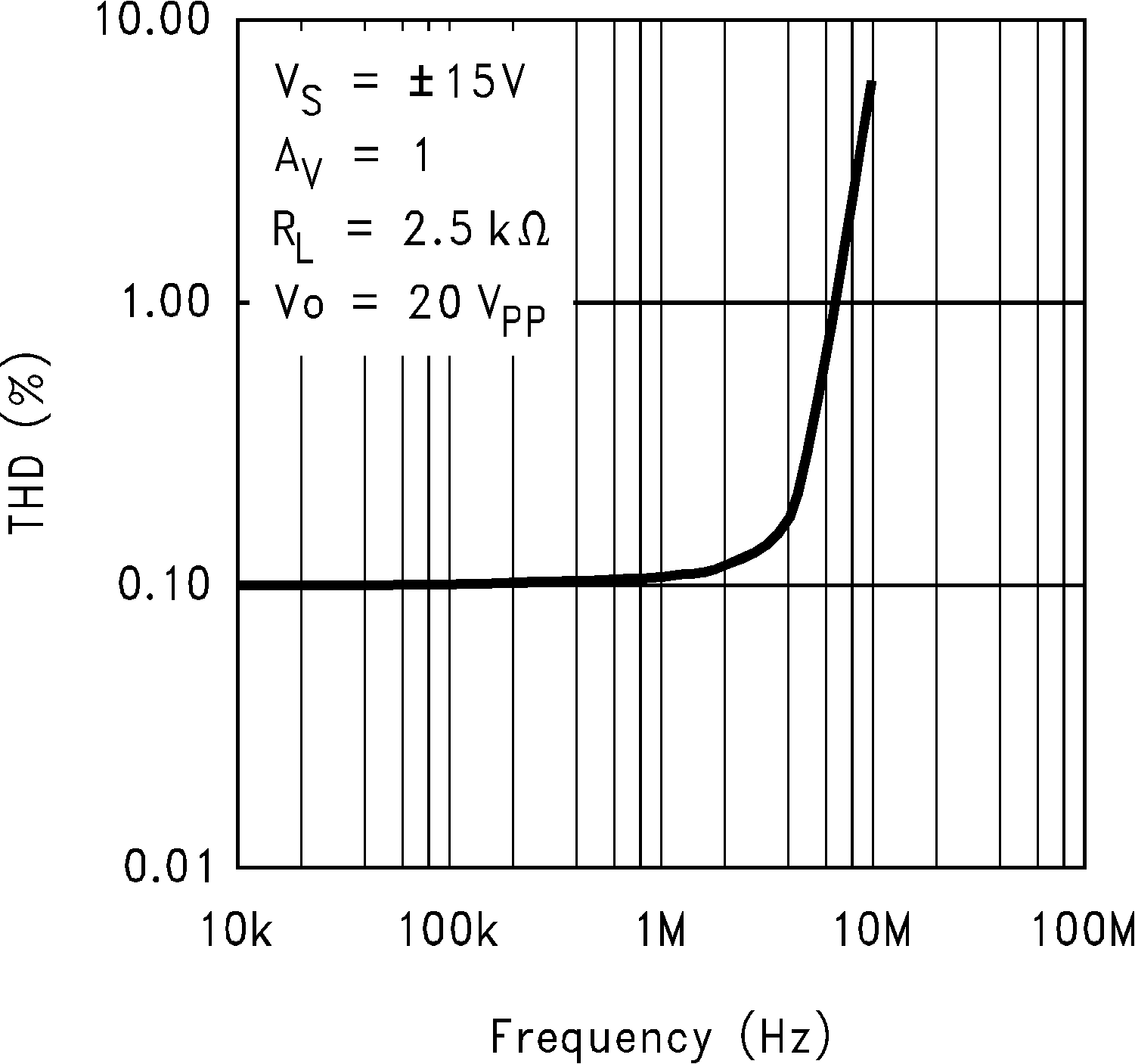
| T.H.D. | Total Harmonic Distortion | 2 VPP Output, RL = 150 Ω, AV = +2, f = 1 MHz |
0.1% | ||
| 2 VPP Output, RL = 150 Ω, AV = +2, f = 5 MHz |
0.6 |
6.9 +5V DC Electrical Characteristics
Unless otherwise specified, all limits ensured for V+ = +5V, V− = 0 V, VCM = VO = V+/2 and RL > 1 MΩ. Boldface limits apply at the temperature extremes.| PARAMETER | TEST CONDITIONS | TYP(4) | LM7121I LIMIT(5) |
UNIT | |
|---|---|---|---|---|---|
| VOS | Input Offset Voltage | 2.4 | mV | ||
| IB | Input Bias Current | 4 | µA | ||
| IOS | Input Offset Current | 0.04 | µA | ||
| RIN | Input Resistance | Common Mode | 2.6 | M | |
| Differential Mode | 3.4 | M | |||
| CIN | Input Capacitance | Common Mode | 2.3 | pF | |
| CMRR | Common Mode Rejection Ratio | 2V ≤ VCM ≤ 3V | 65 | dB | |
| +PSRR | Positive Power Supply Rejection Ratio | 4.6V ≤ V+ ≤ 5V | 85 | dB | |
| −PSRR | Negative Power Supply Rejection Ratio | 0V ≤ V− ≤ 0.4V | 61 | dB | |
| VCM | Input Common-Mode Voltage Range | CMRR 45 dB | 3.5 | V min | |
| 1.5 | V max | ||||
| AV | Large Signal Voltage Gain | RL = 2 kΩ to V+/2 | 64 | dB | |
| VO | Output Swing | RL = 2 kΩ to V+/2, High | 3.7 | V | |
| RL = 2 kΩ to V+/2, Low | 1.3 | ||||
| RL = 150 Ω to V+/2, High | 3.48 | ||||
| RL = 150 Ω to V+/2, Low | 1.59 | ||||
| ISC | Output Short Circuit Current | Sourcing | 33 | mA | |
| Sinking | 20 | mA | |||
| IS | Supply Current | 4.8 | mA |
6.10 +5V AC Electrical Characteristics
Unless otherwise specified, all limits ensured for V+ = +5V, V− = 0 V, VCM = VO = V+/2 and RL > 1 MΩ. Boldface limits apply at the temperature extremes.| PARAMETER | TEST CONDITIONS | TYP(4) | LM7121I LIMIT(5) |
UNIT | |
|---|---|---|---|---|---|
| SR | Slew Rate(6) | AV = +2, RL = 1 kΩ to V+/2, VO = 1.8 VPP |
145 | V/µs | |
| GBW | Unity Gain-Bandwidth | RL = 1k to V+/2 | 80 | MHz | |
| Øm | Phase Margin | RL = 1k to V+/2 | 70 | Deg | |
| f (−3 dB) | Bandwidth(7)(8) | RL = 100 Ω to V+/2, AV = +1 | 200 | MHz | |
| RL = 100 Ω to V+/2, AV = +2 | 45 | ||||
| tr, tf | Rise and Fall Time(8) | AV = +2, RL = 100 Ω , VO = 0.2 VPP | 8 | ns | |
| T.H.D. | Total Harmonic Distortion | 0.6 VPP Output, RL = 150 Ω, AV = +2, f = 1 MHz |
0.067% | ||
| 0.6 VPP Output, RL = 150 Ω, AV = +2, f = 5 MHz |
0.33% |
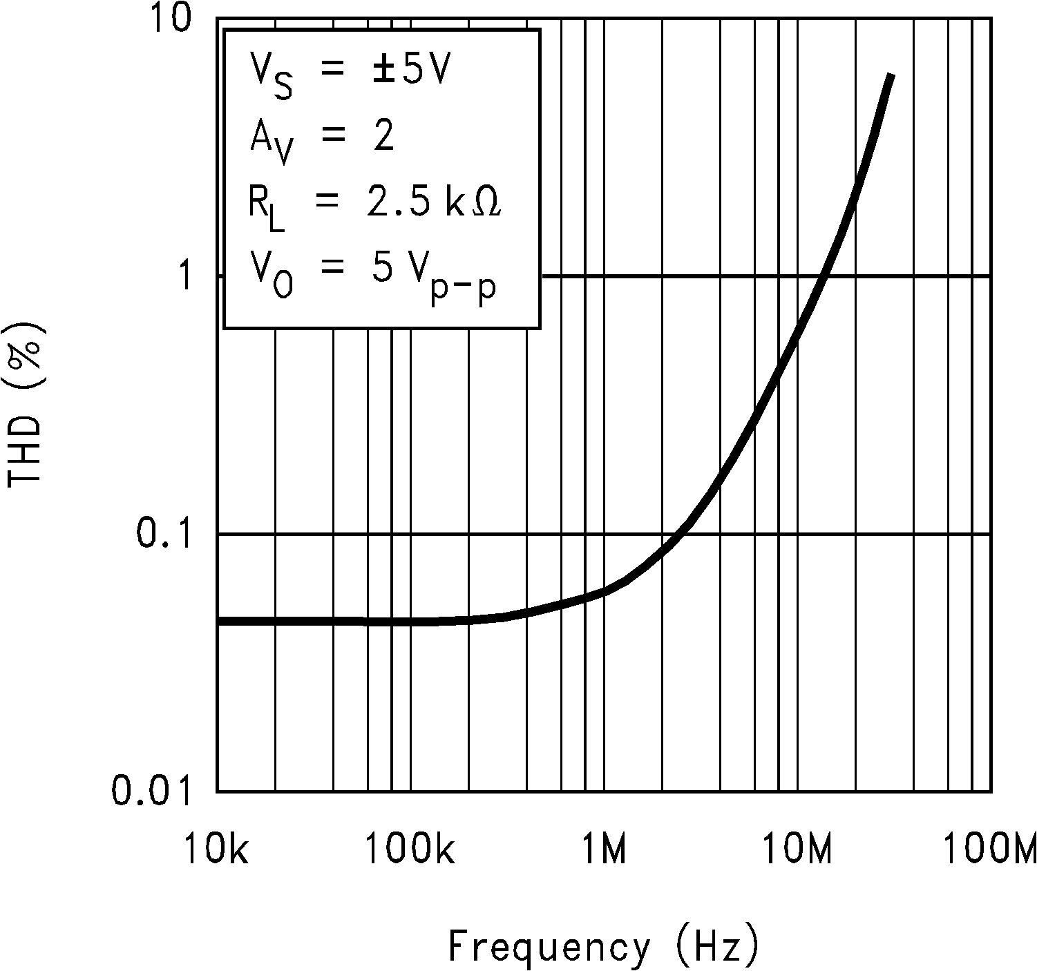
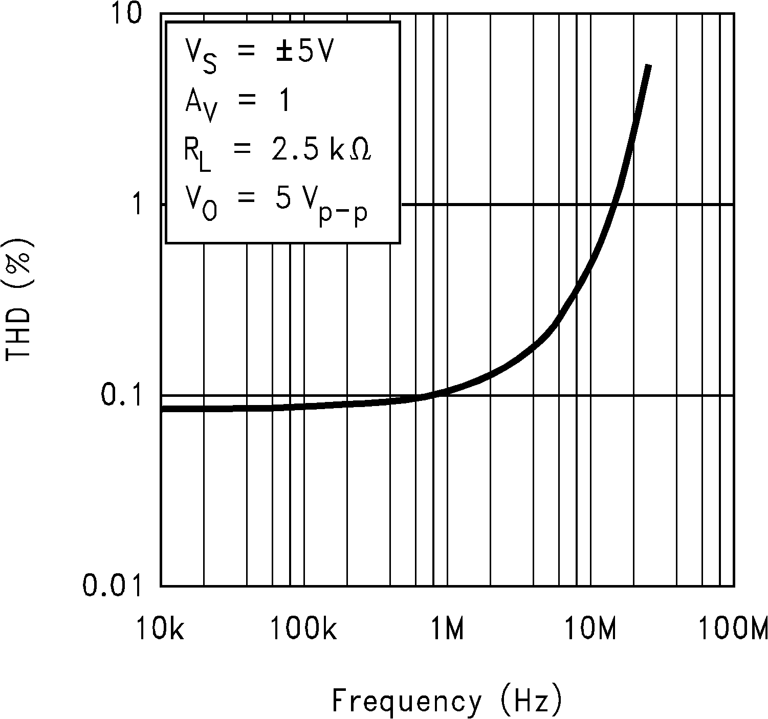
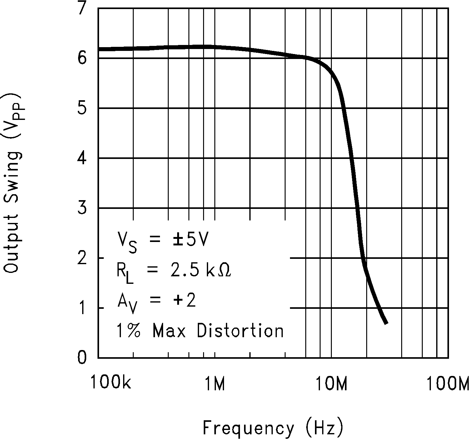
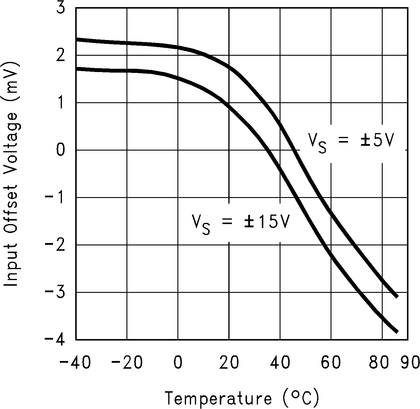
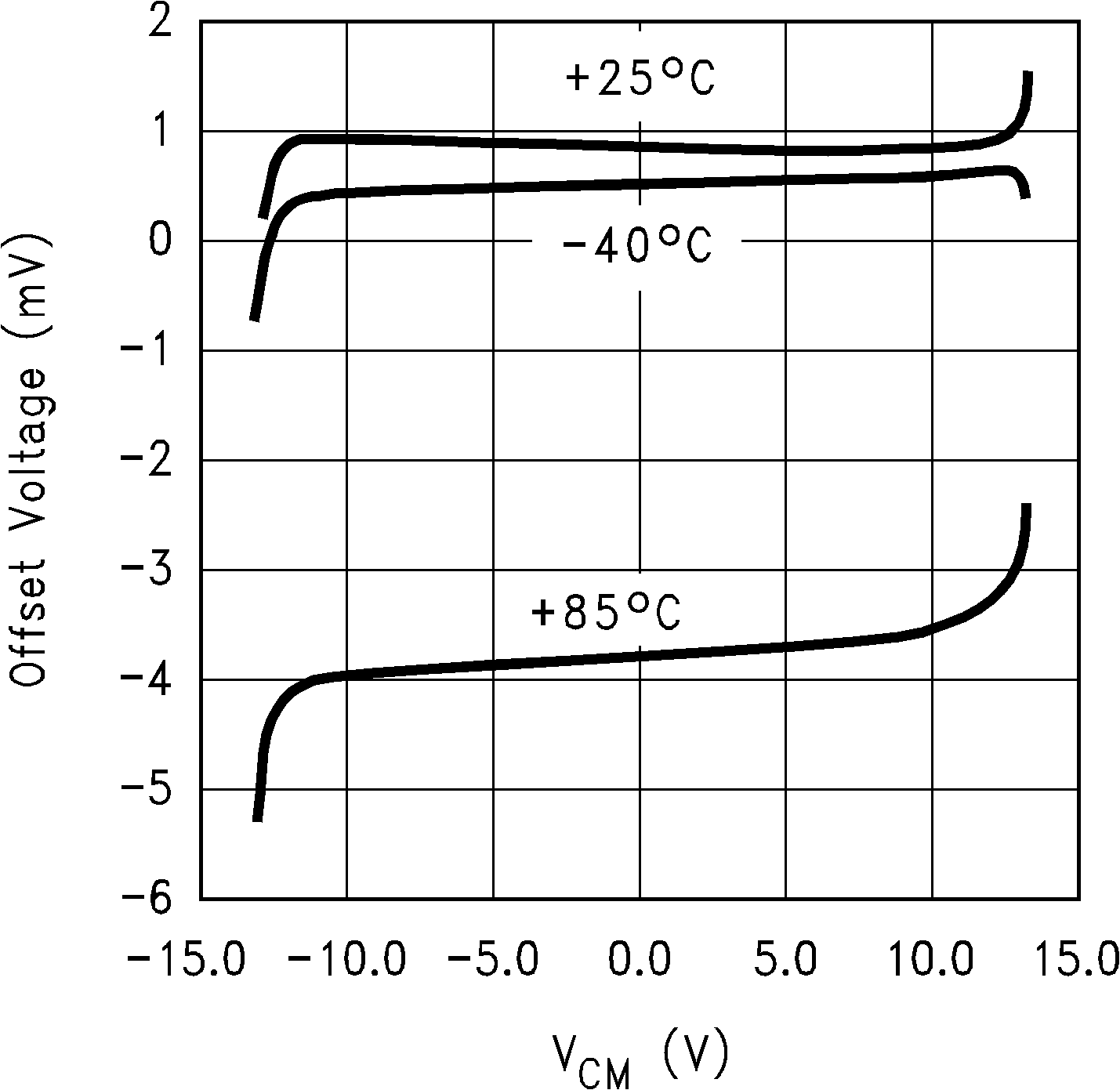
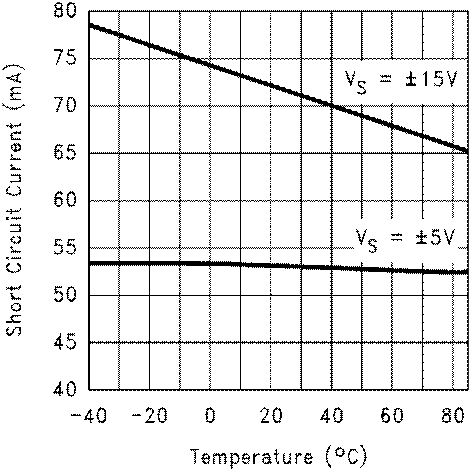
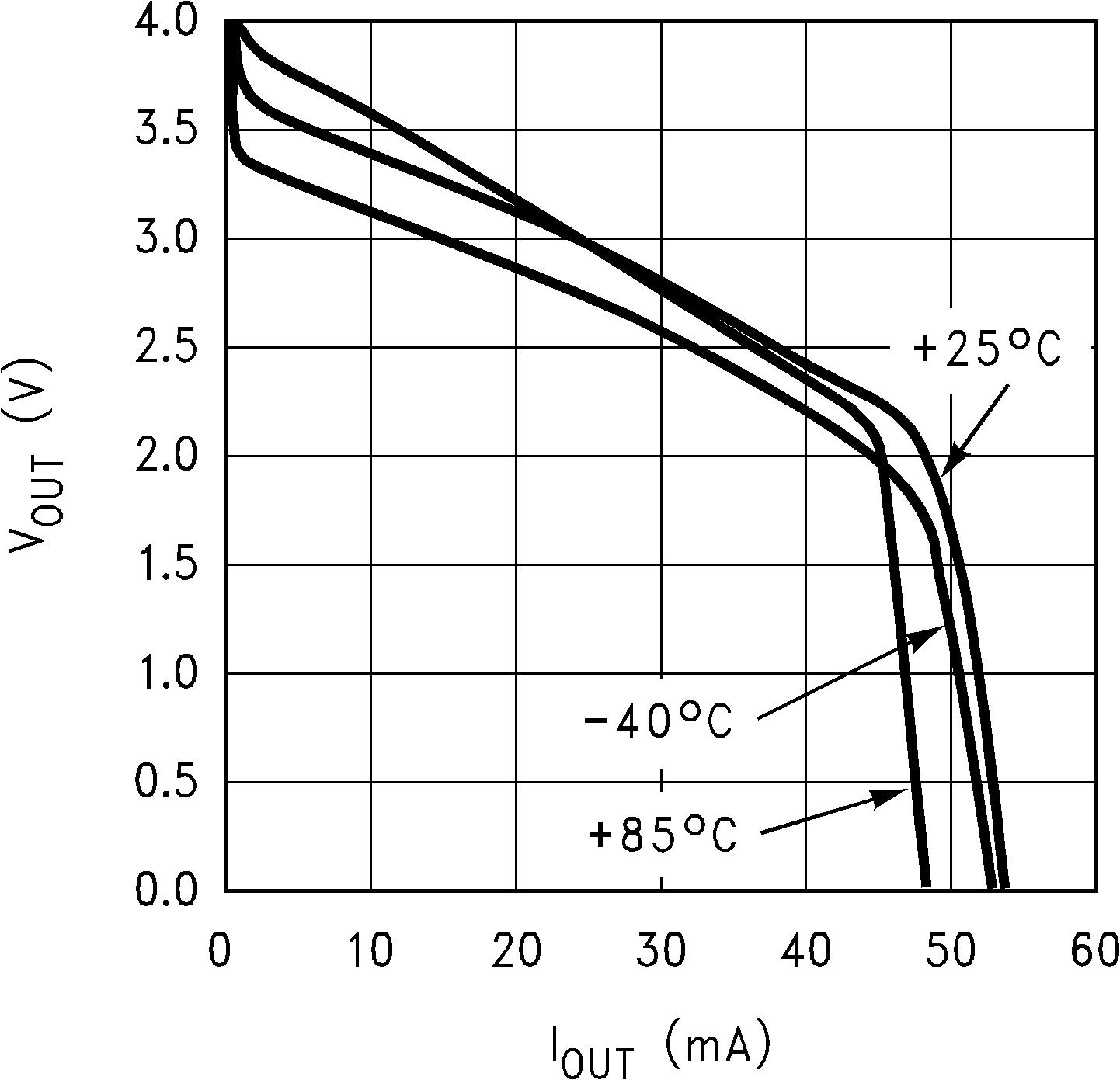
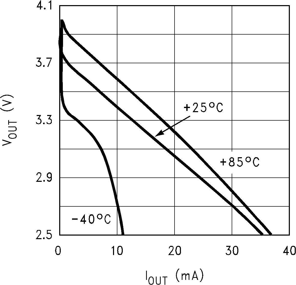
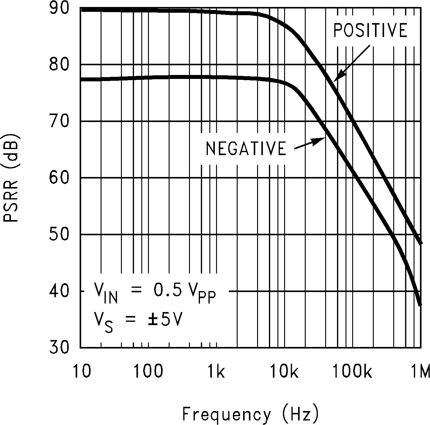
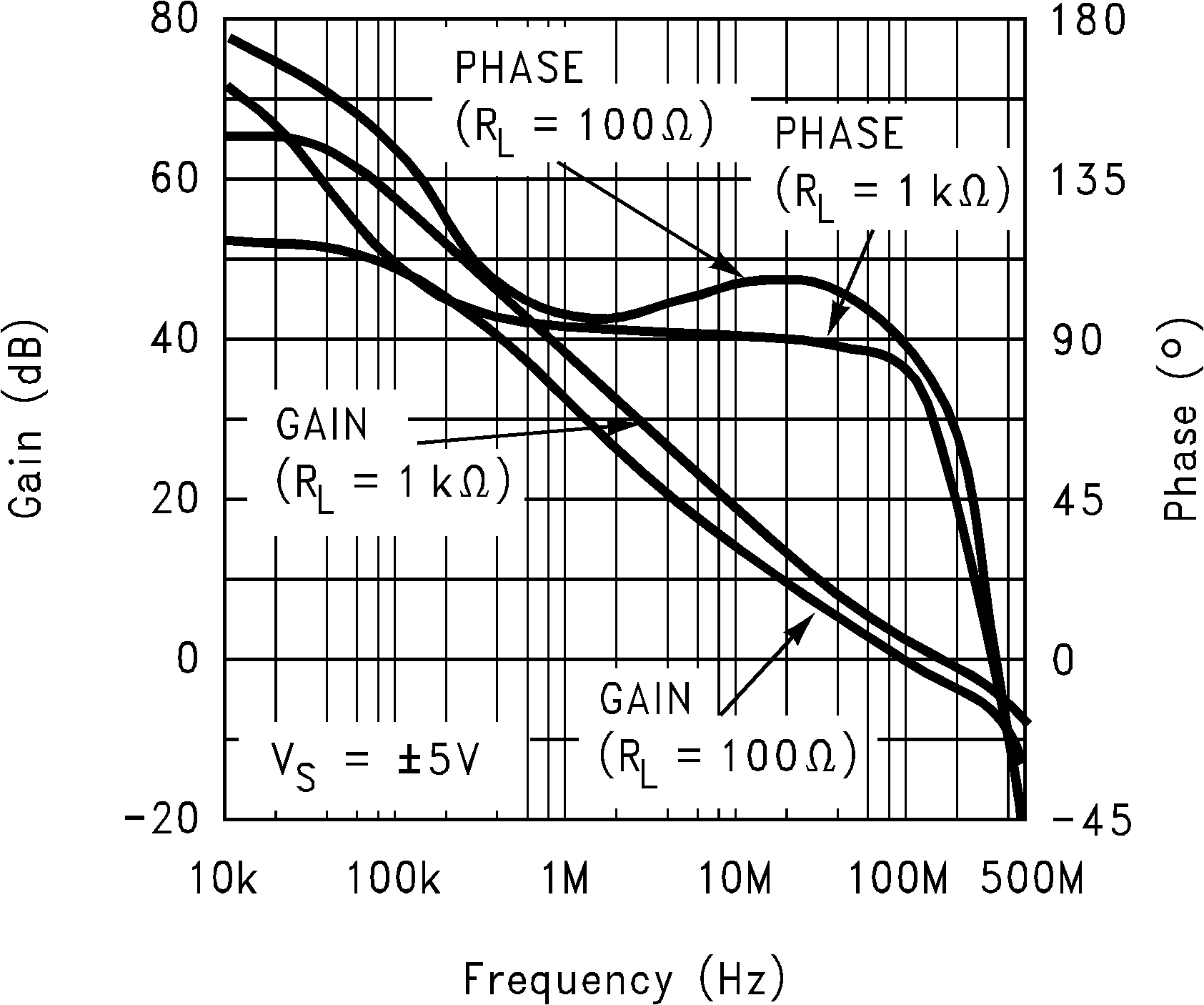
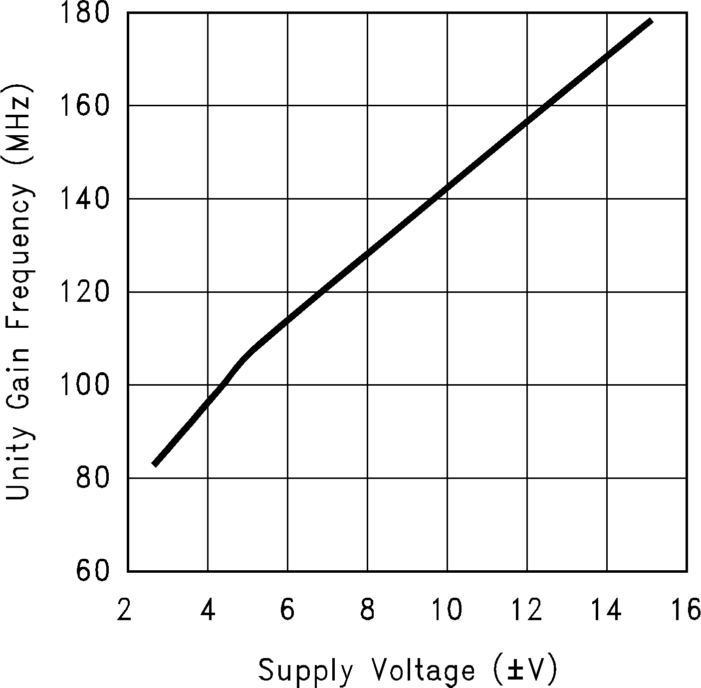
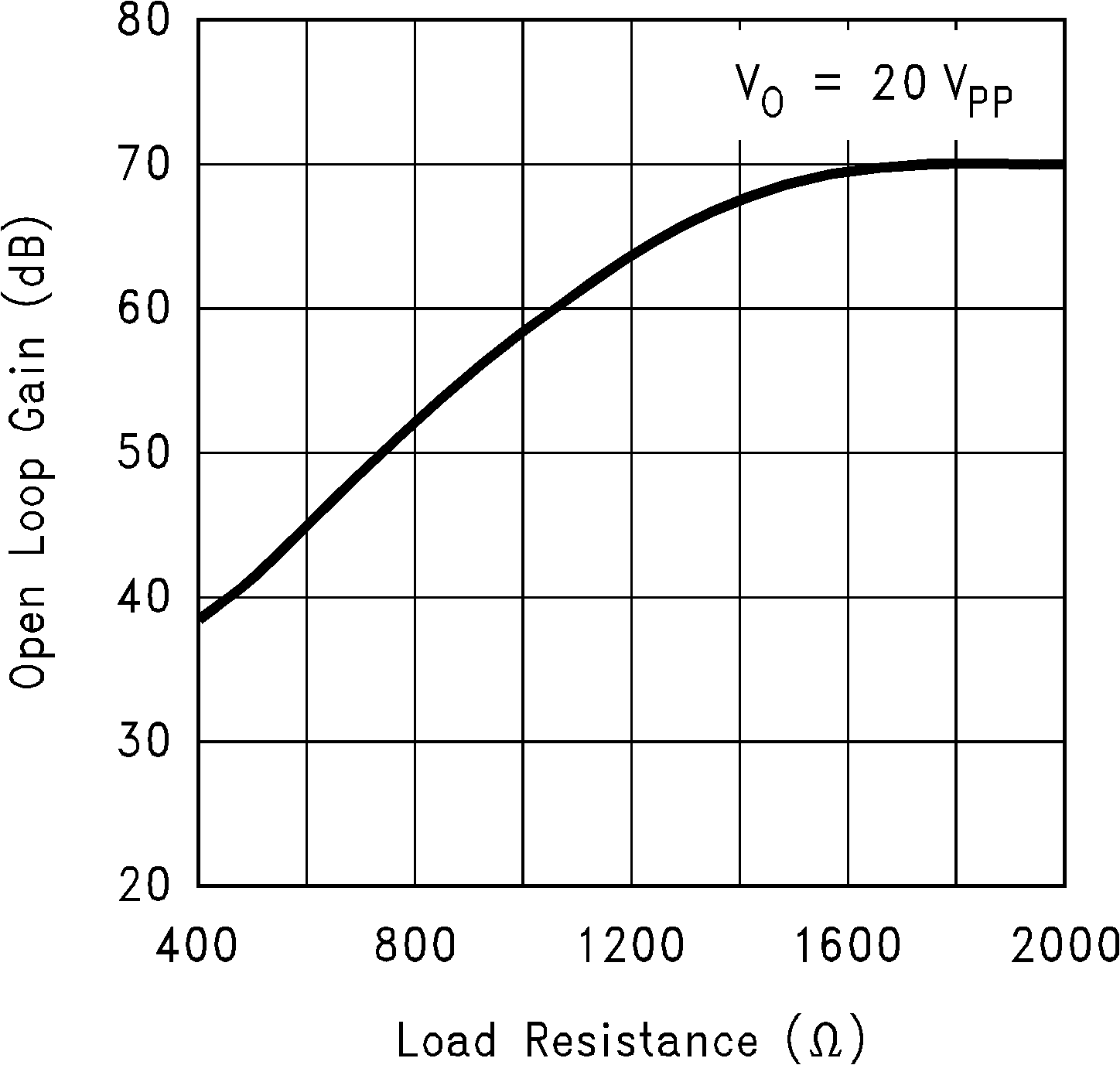
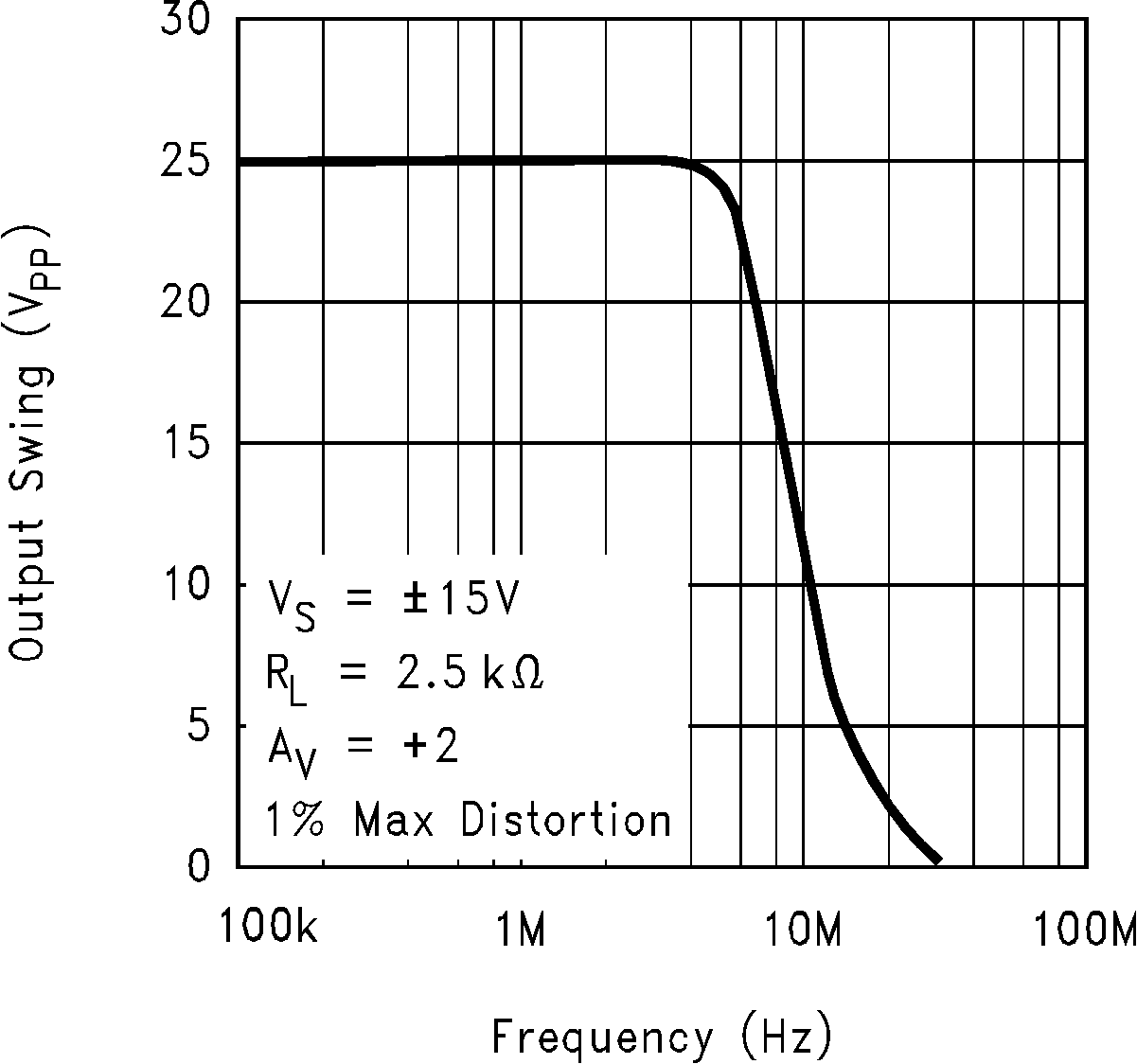
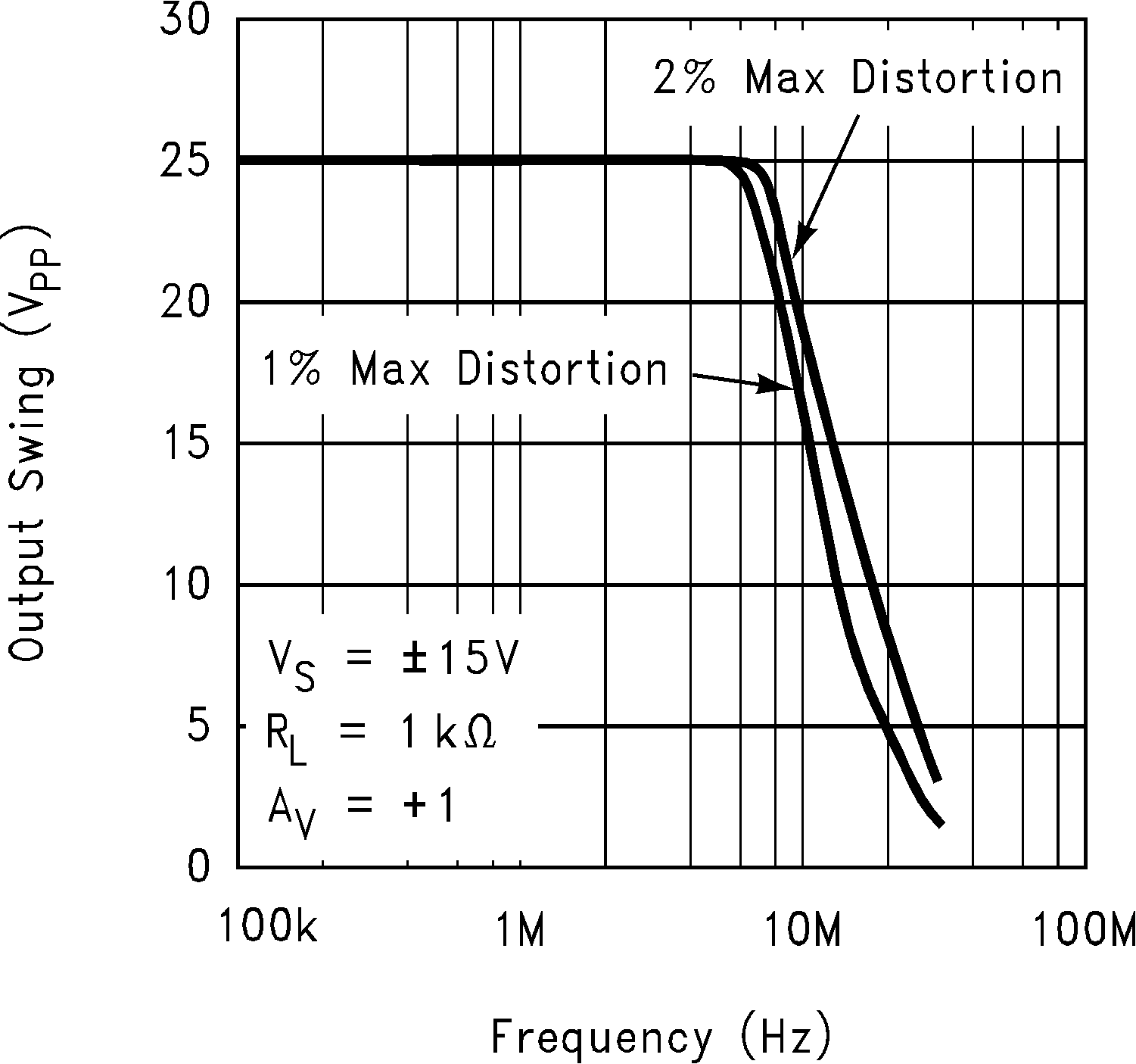
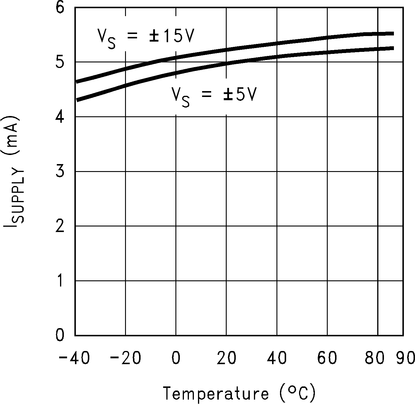
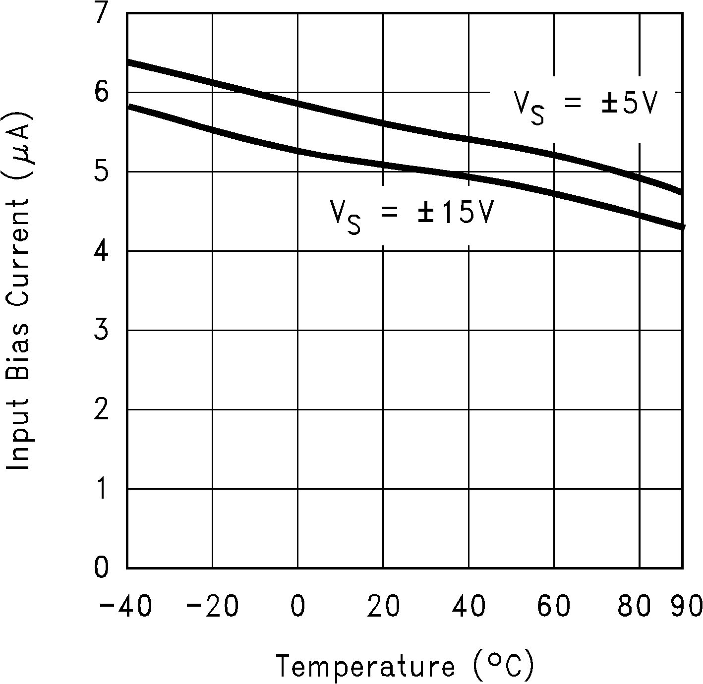
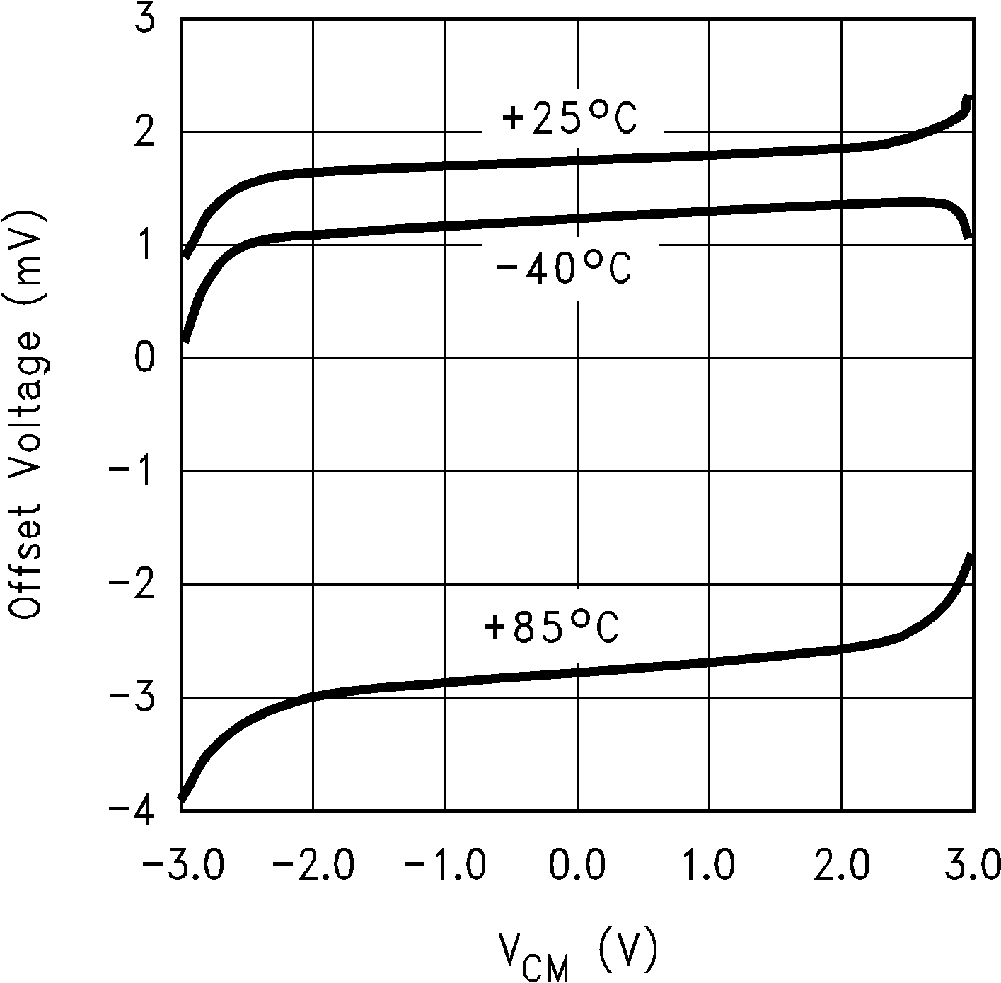
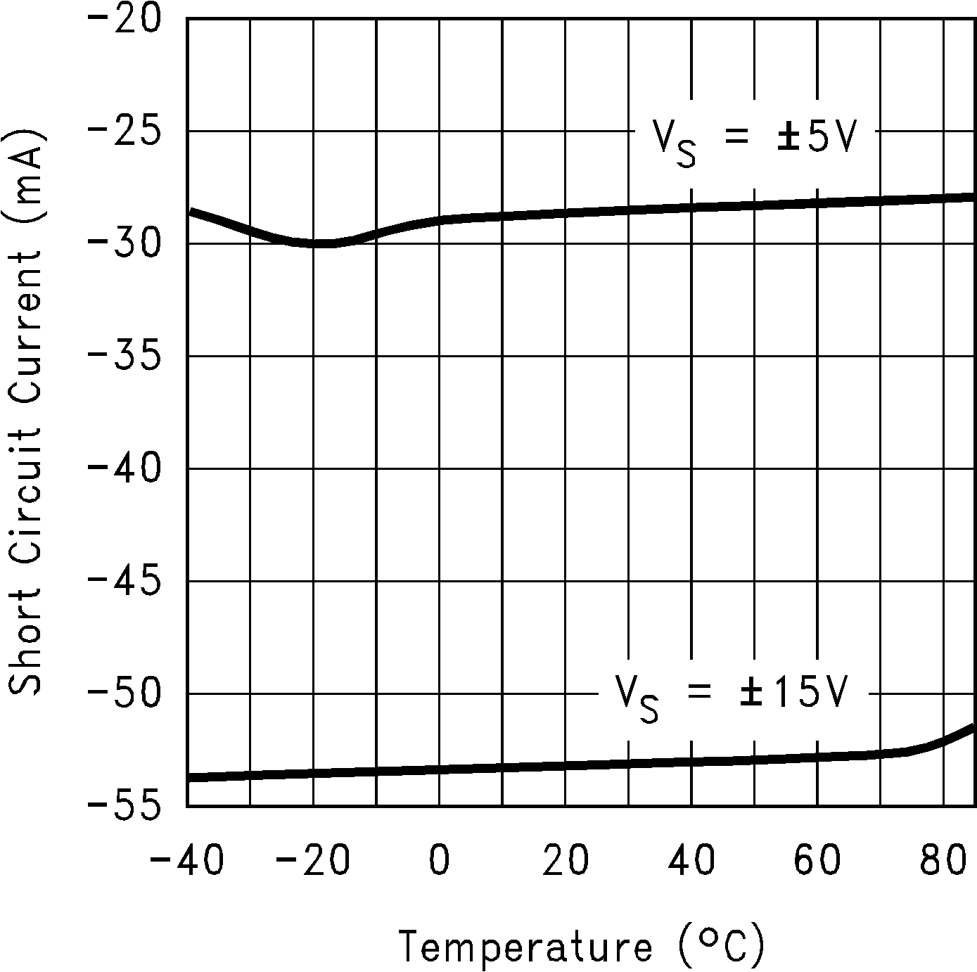
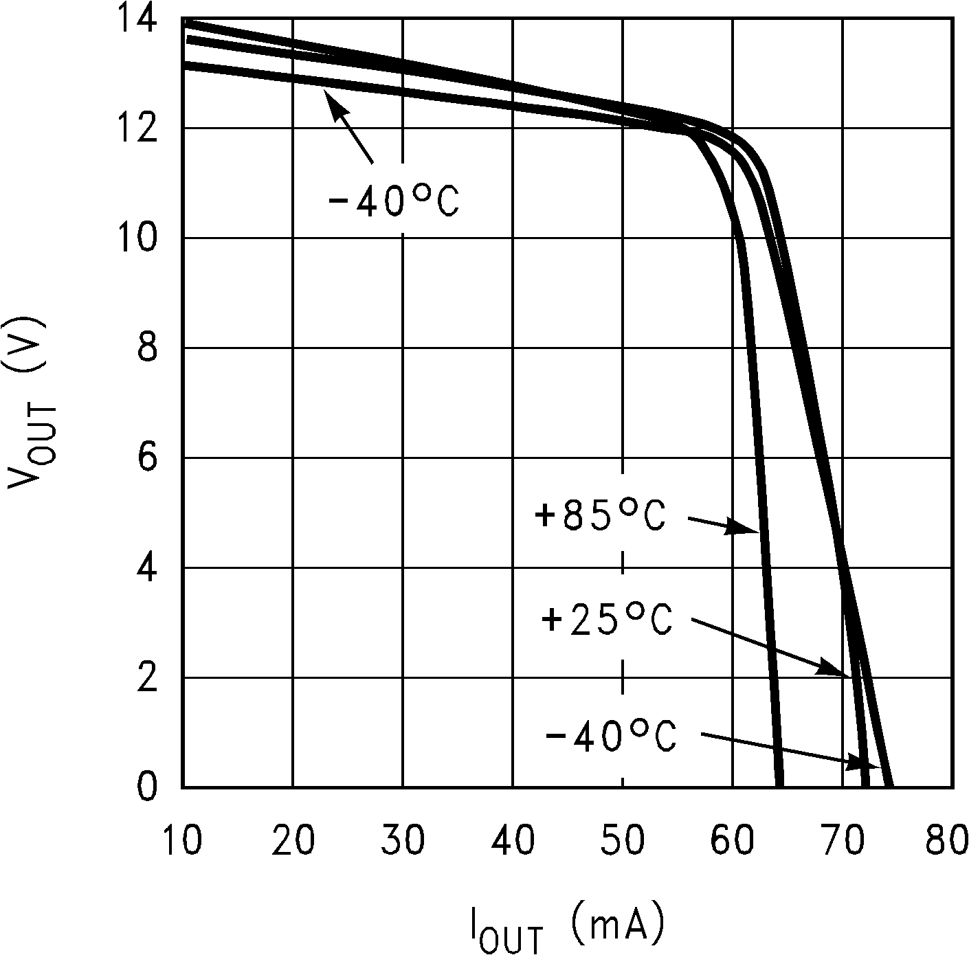
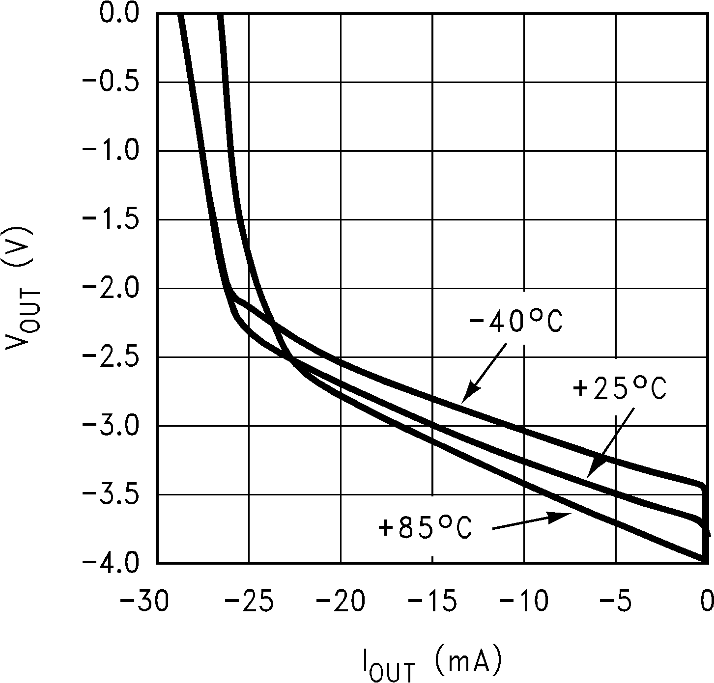
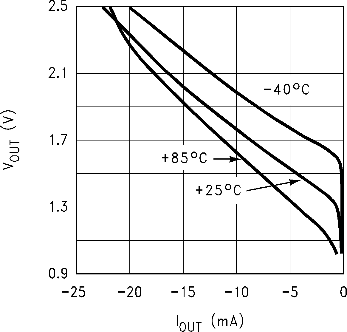
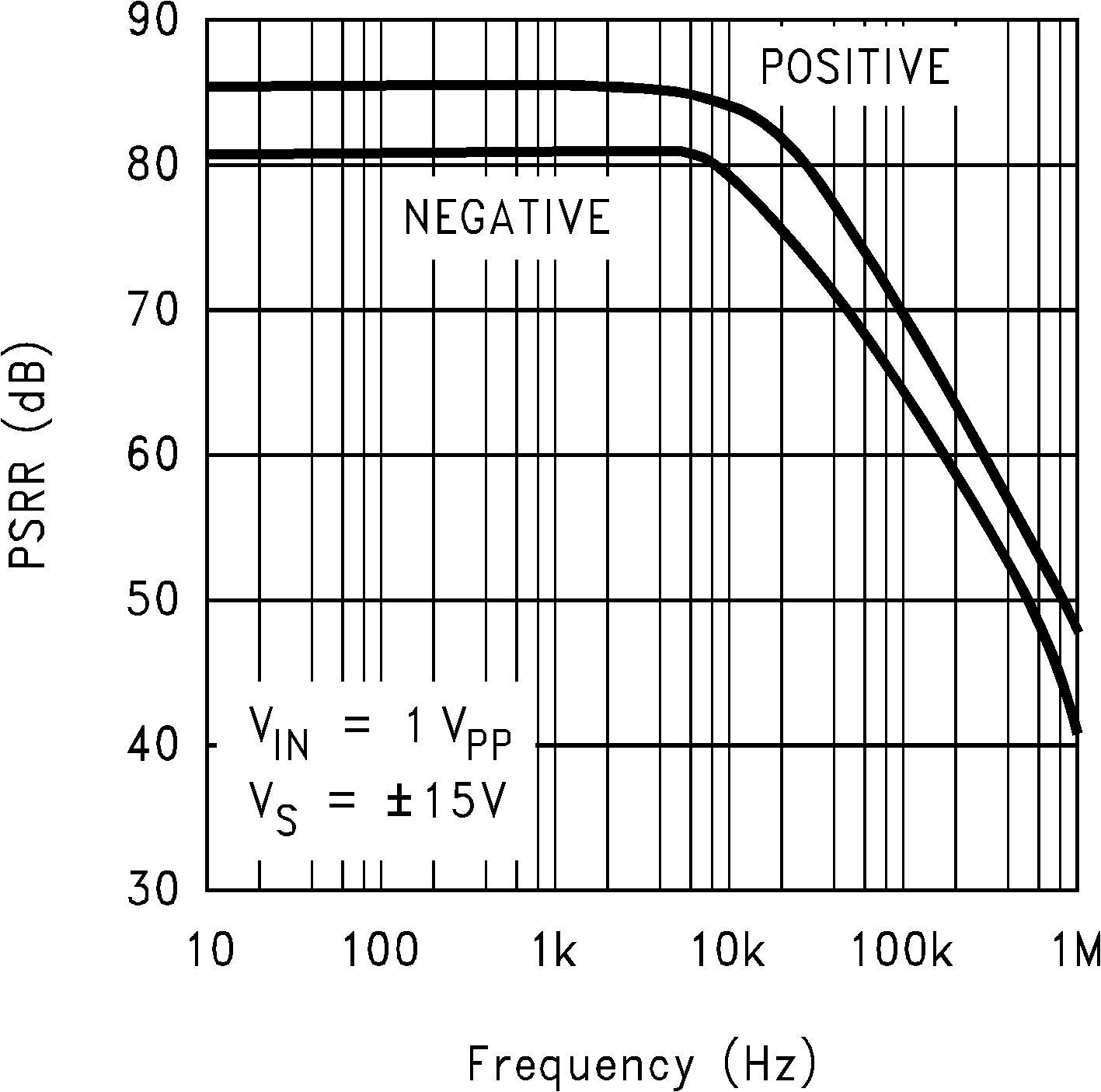
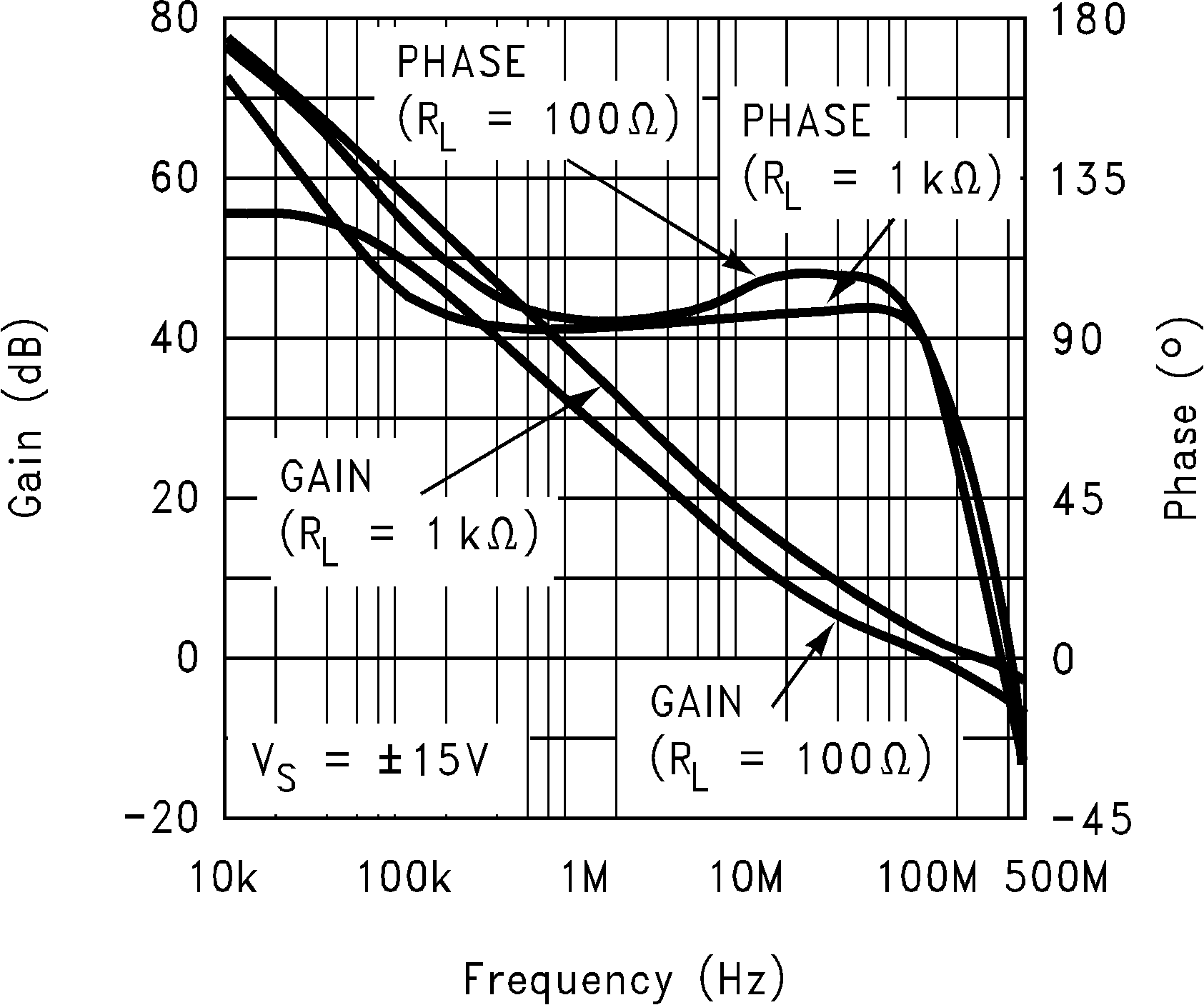
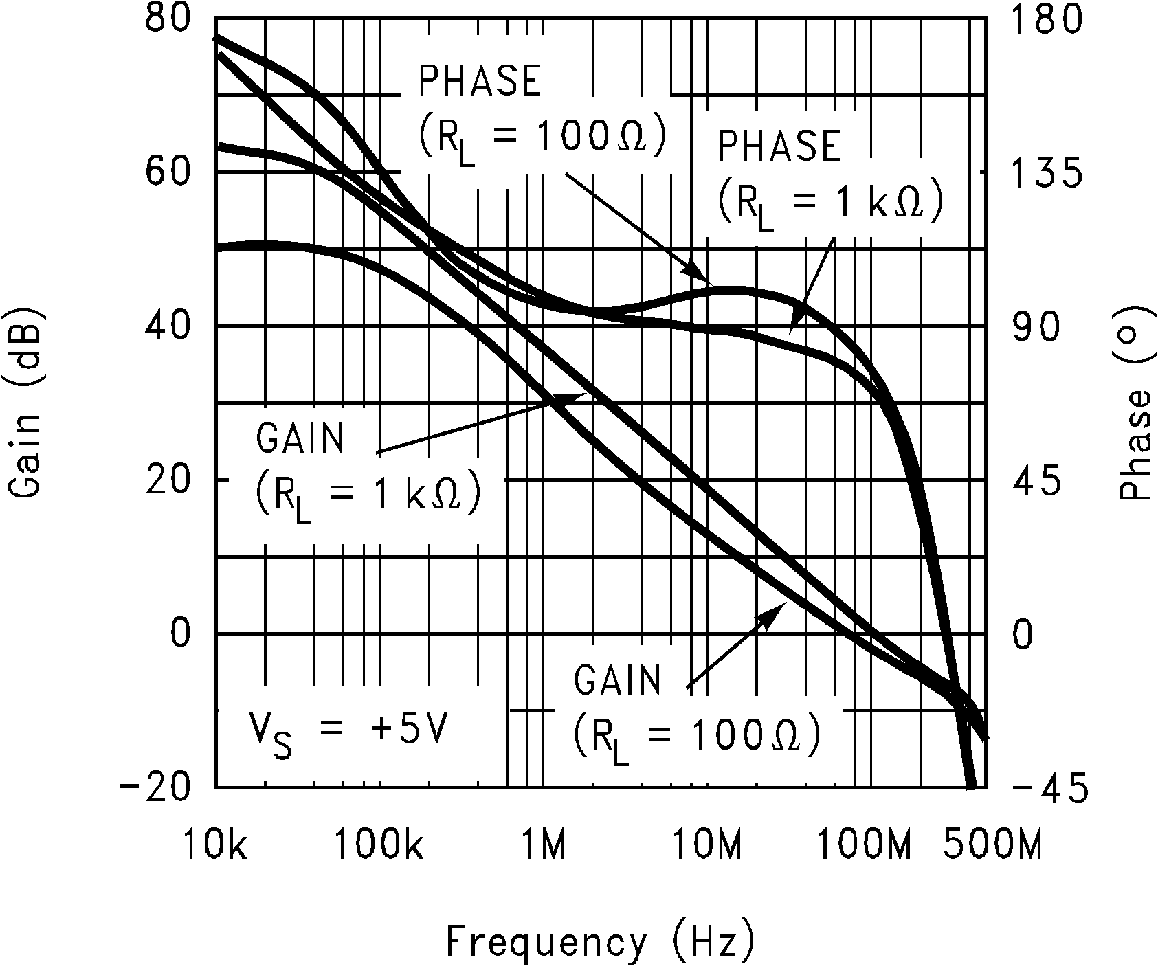
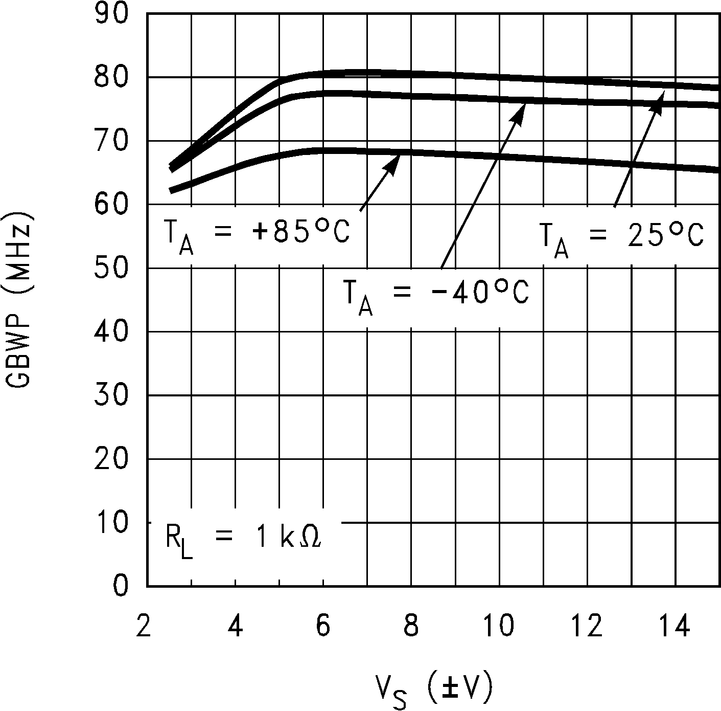
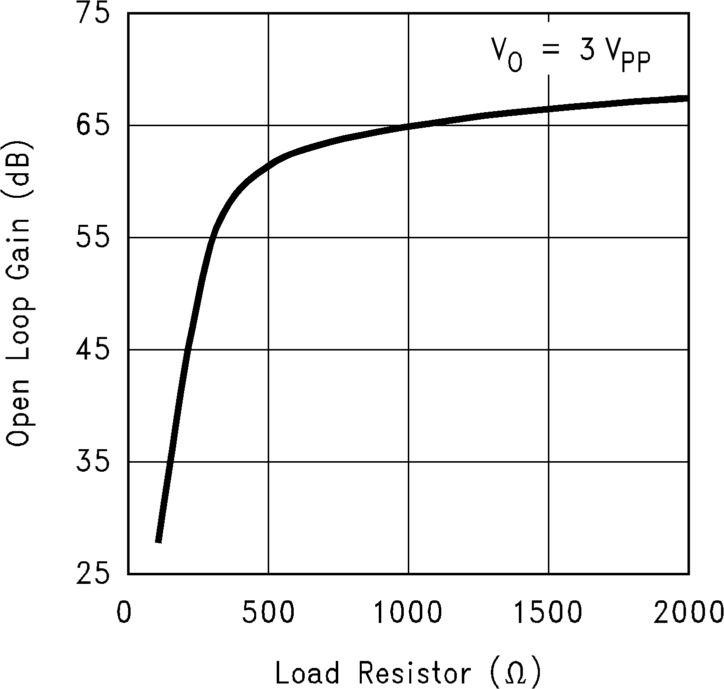
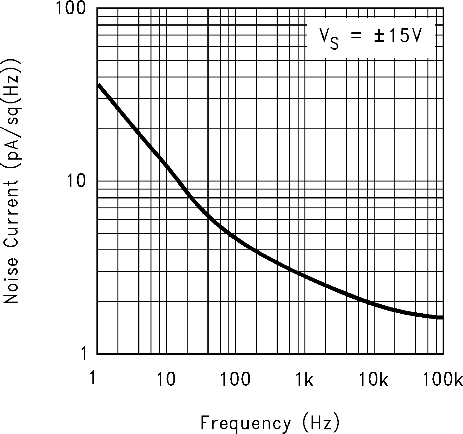
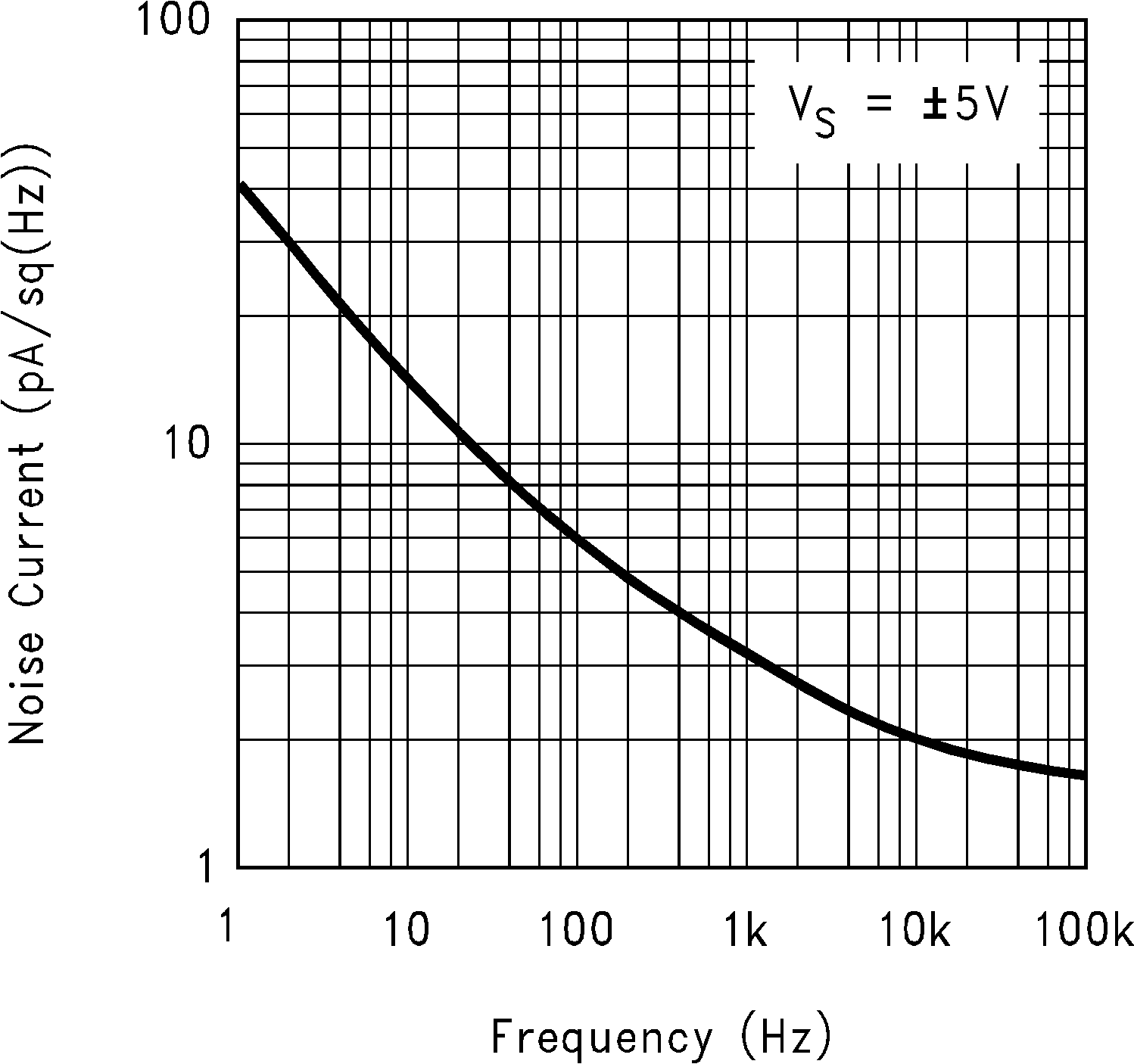
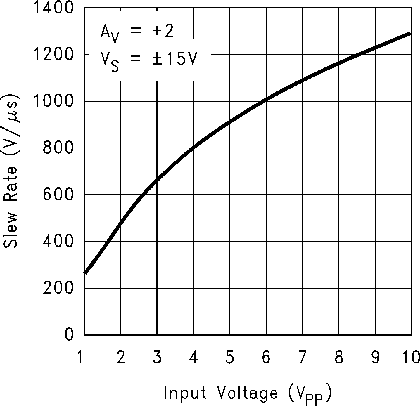
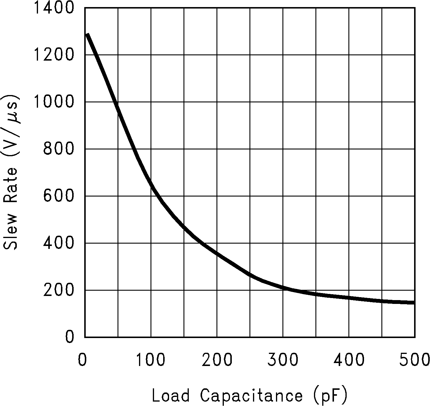
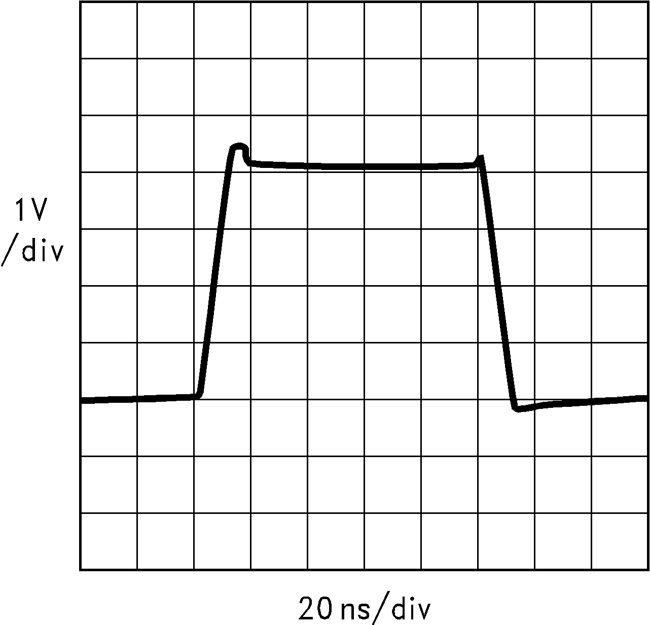
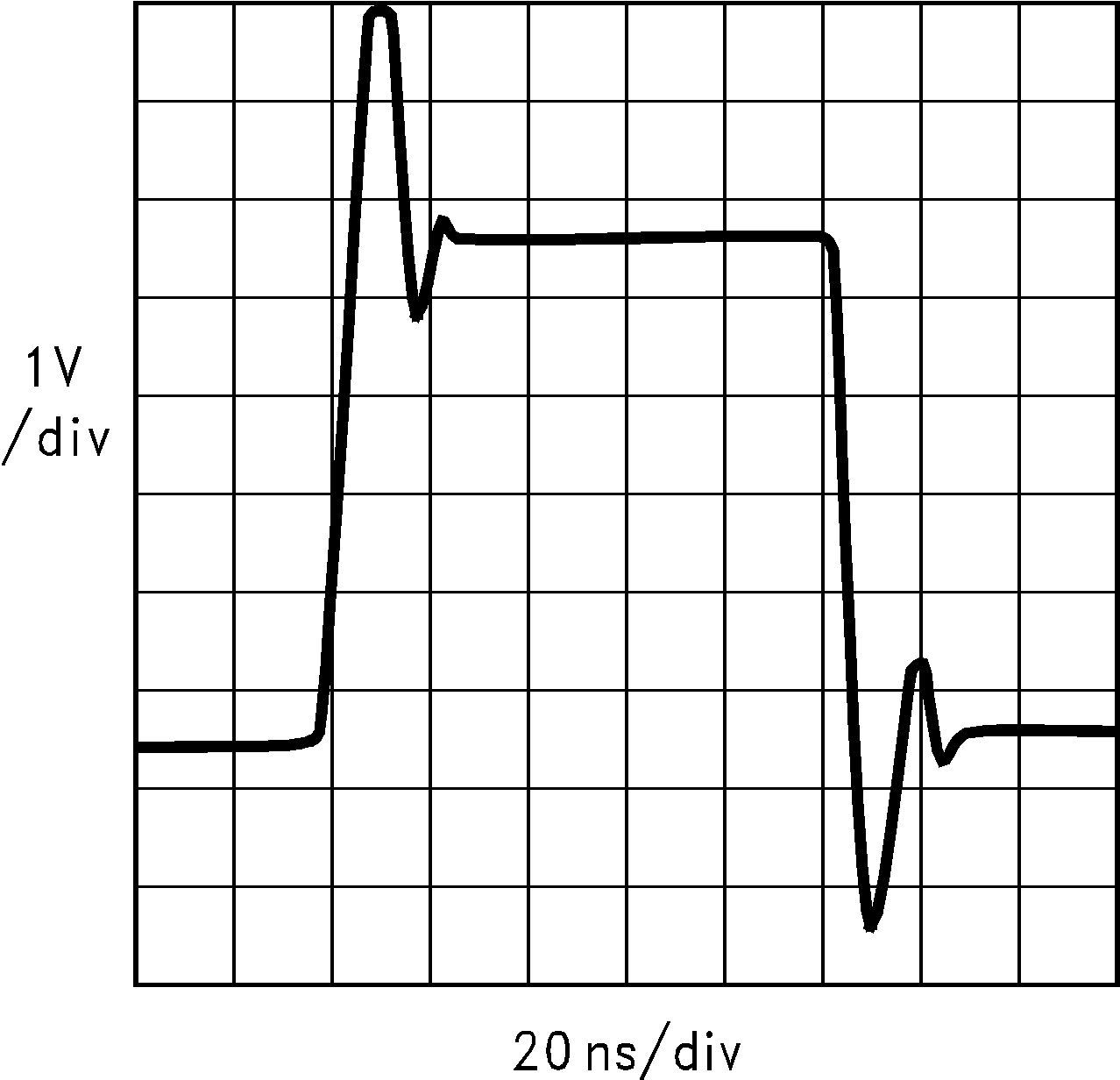
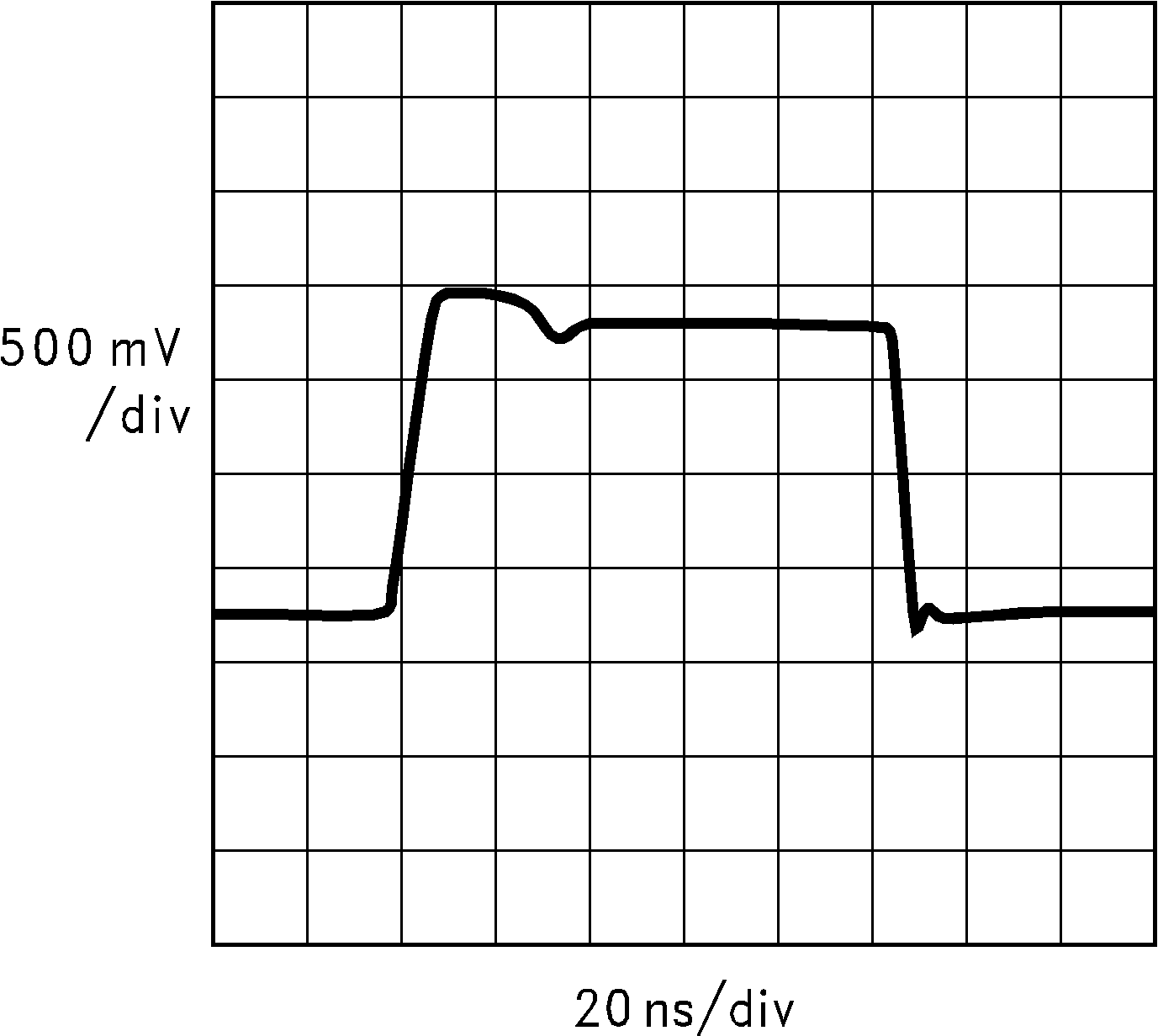
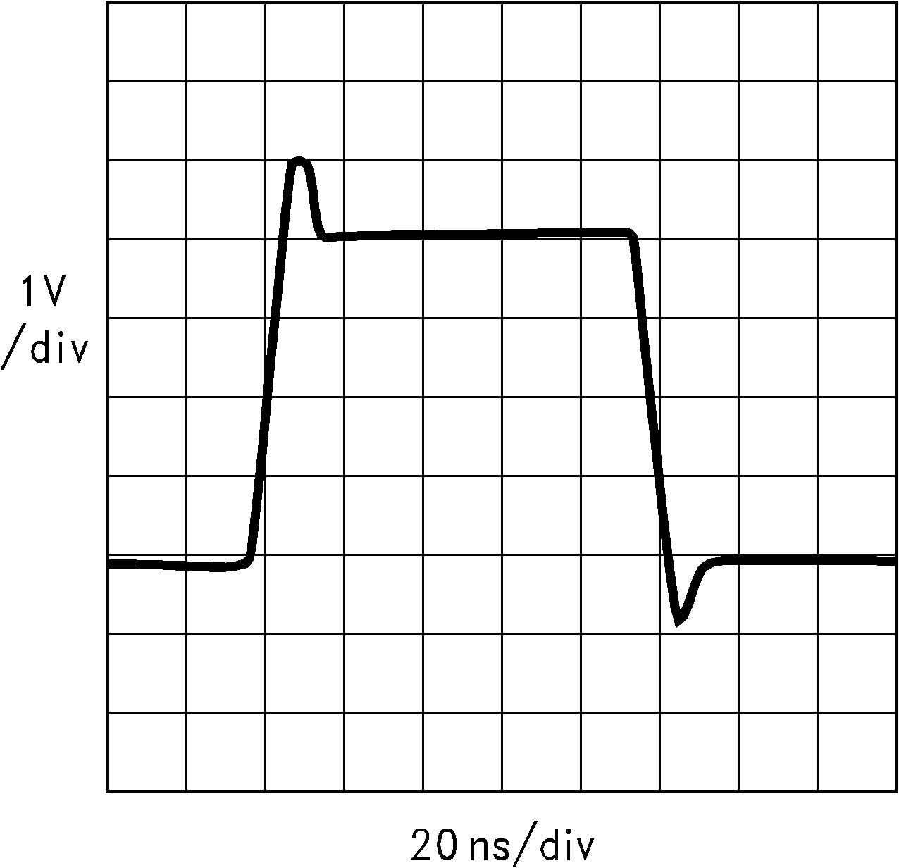
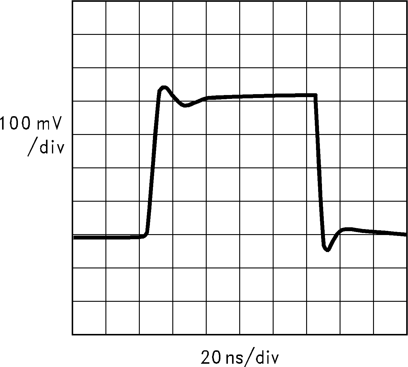
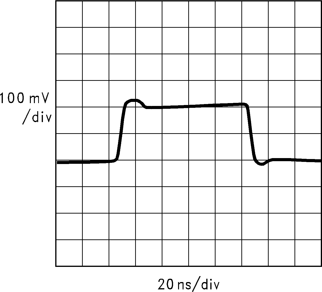
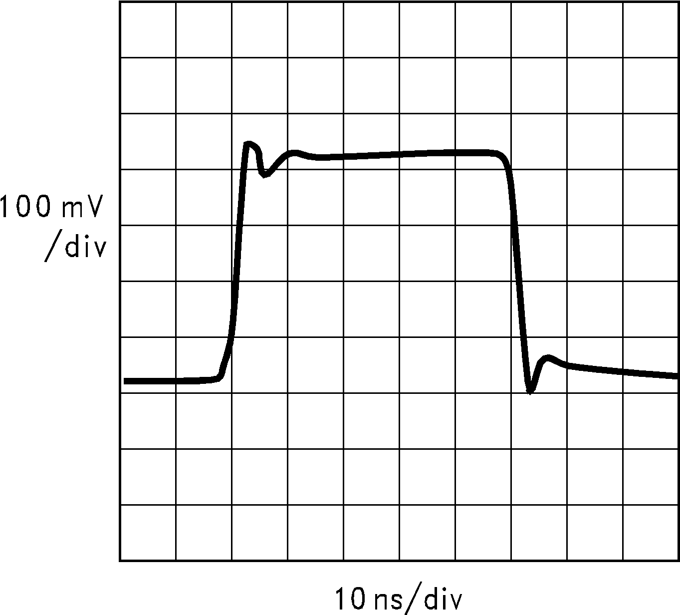
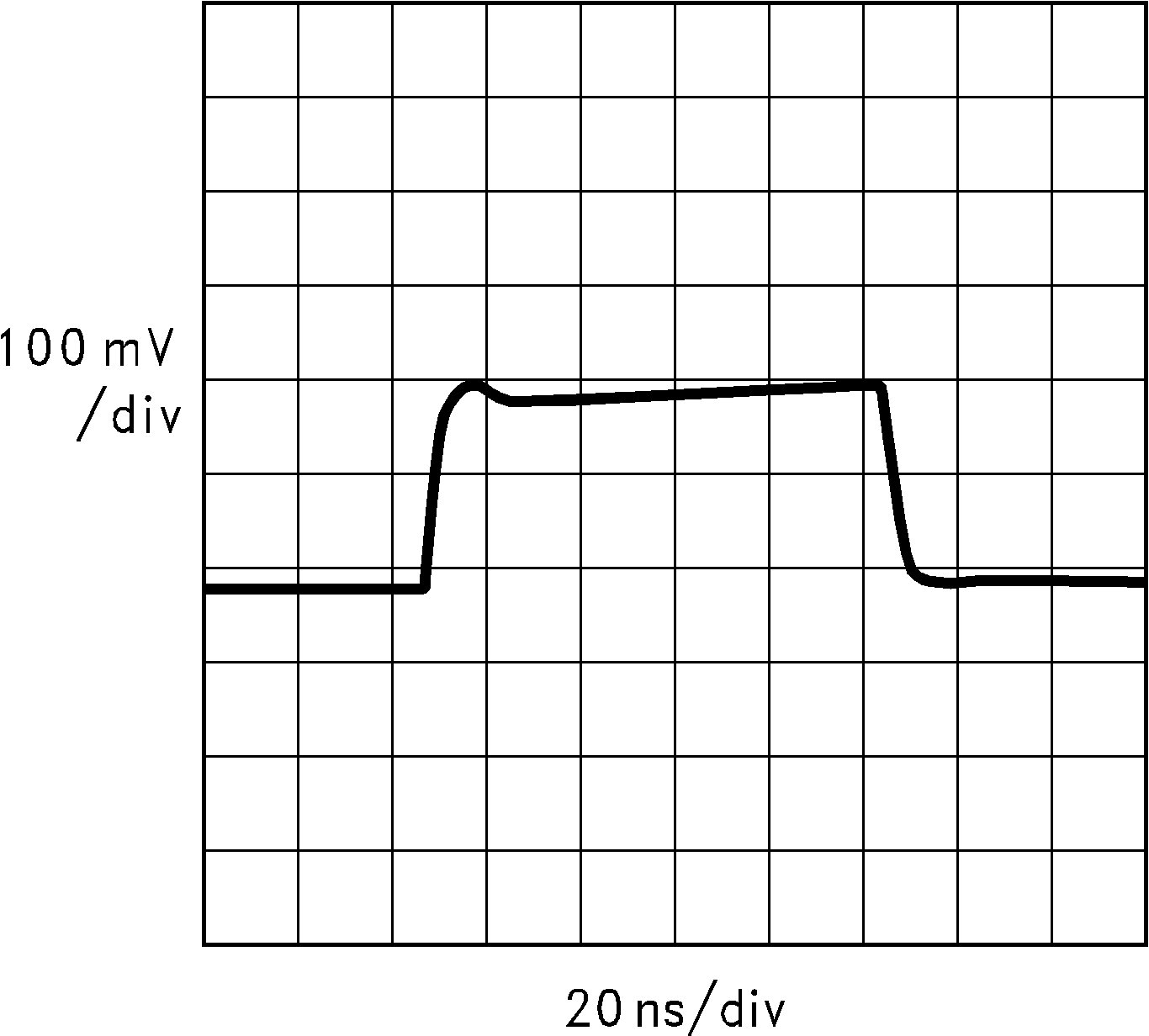
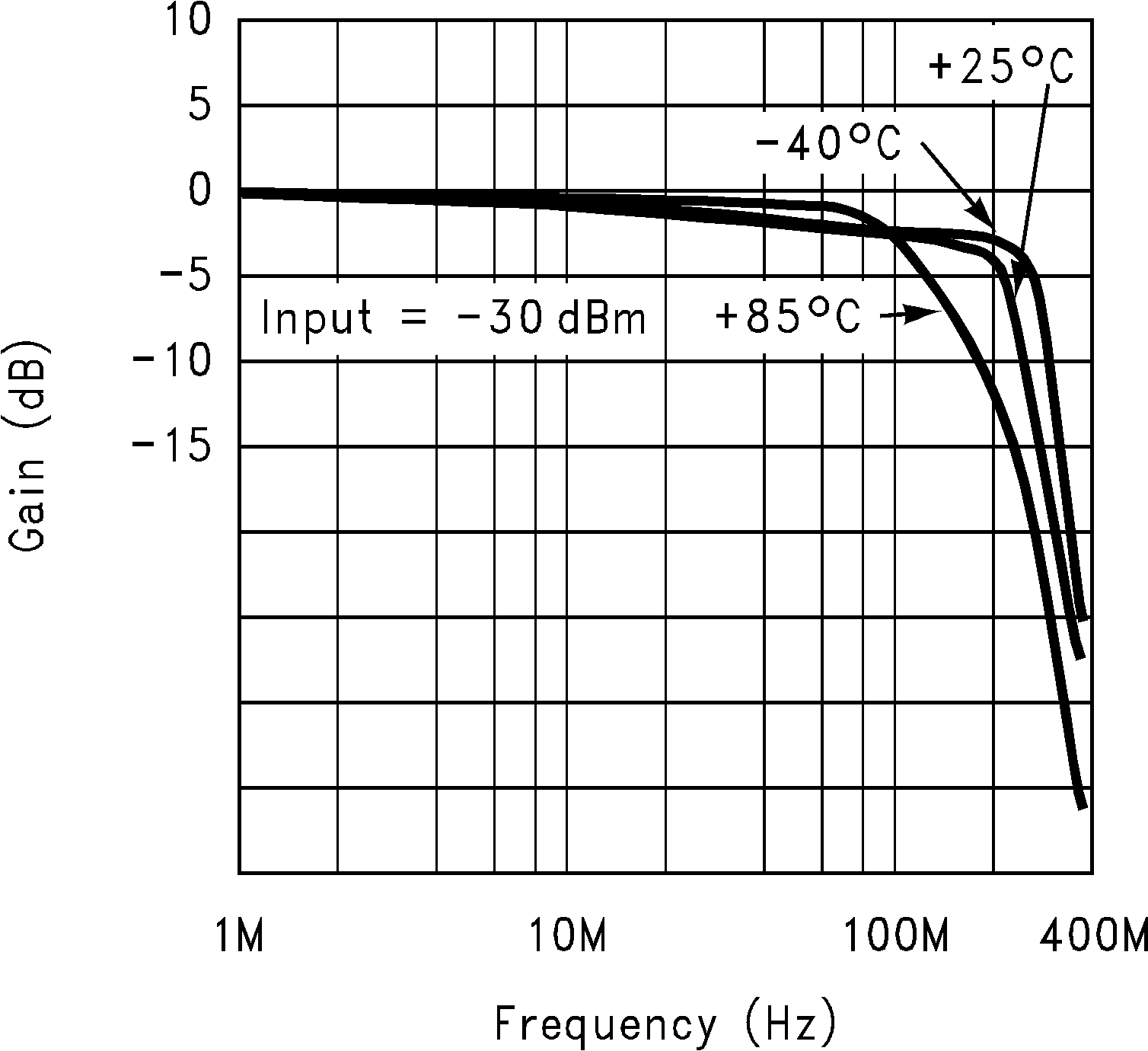
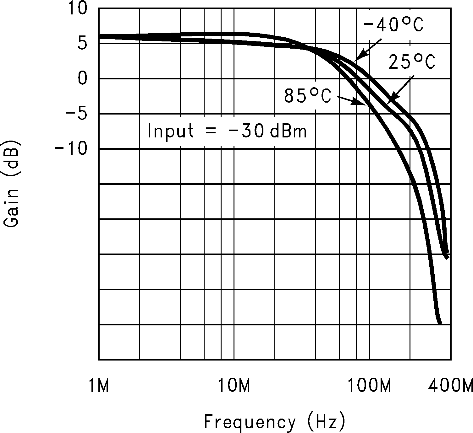
6.11 Typical Characteristics
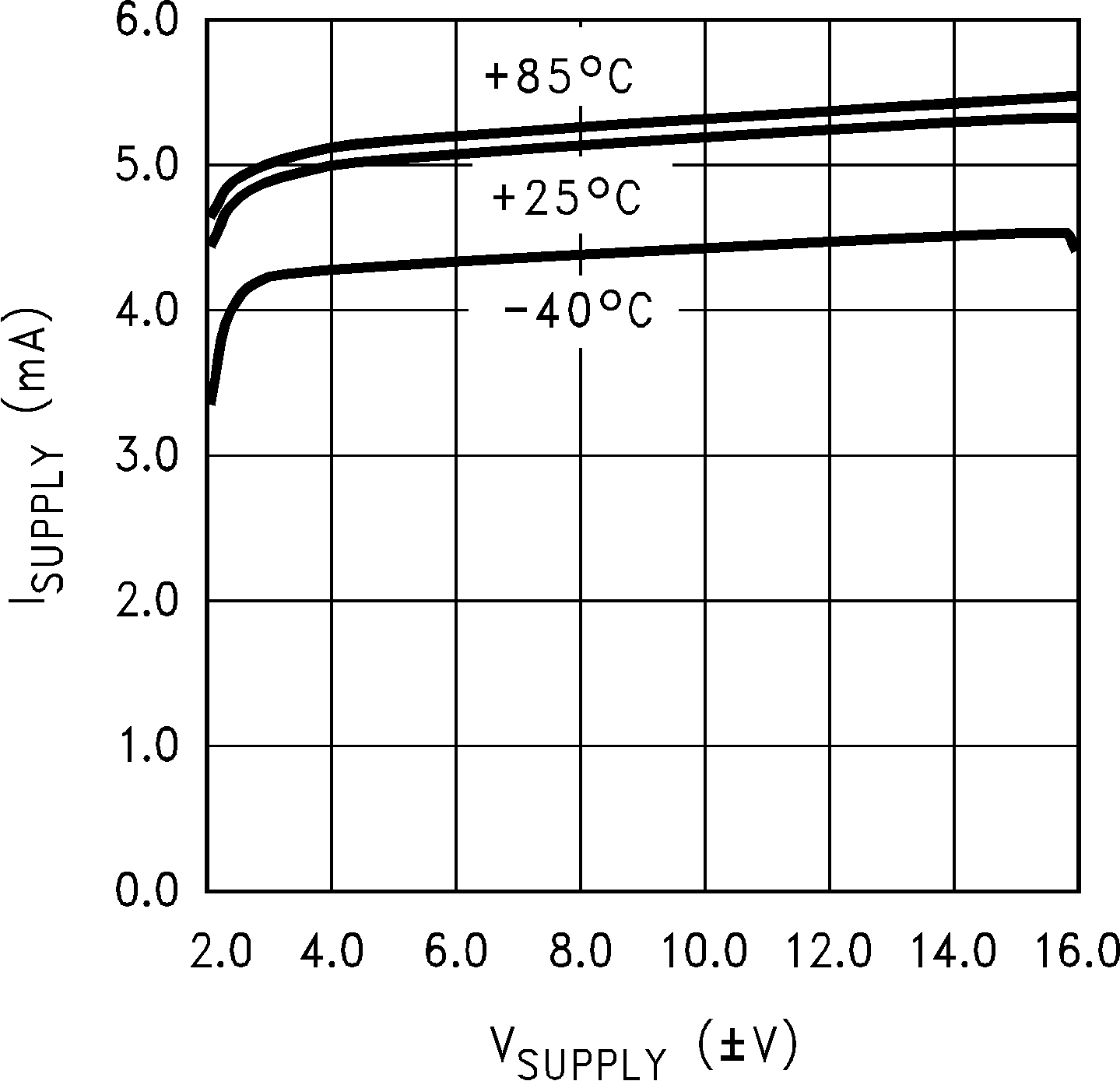
at VS = ±15 V
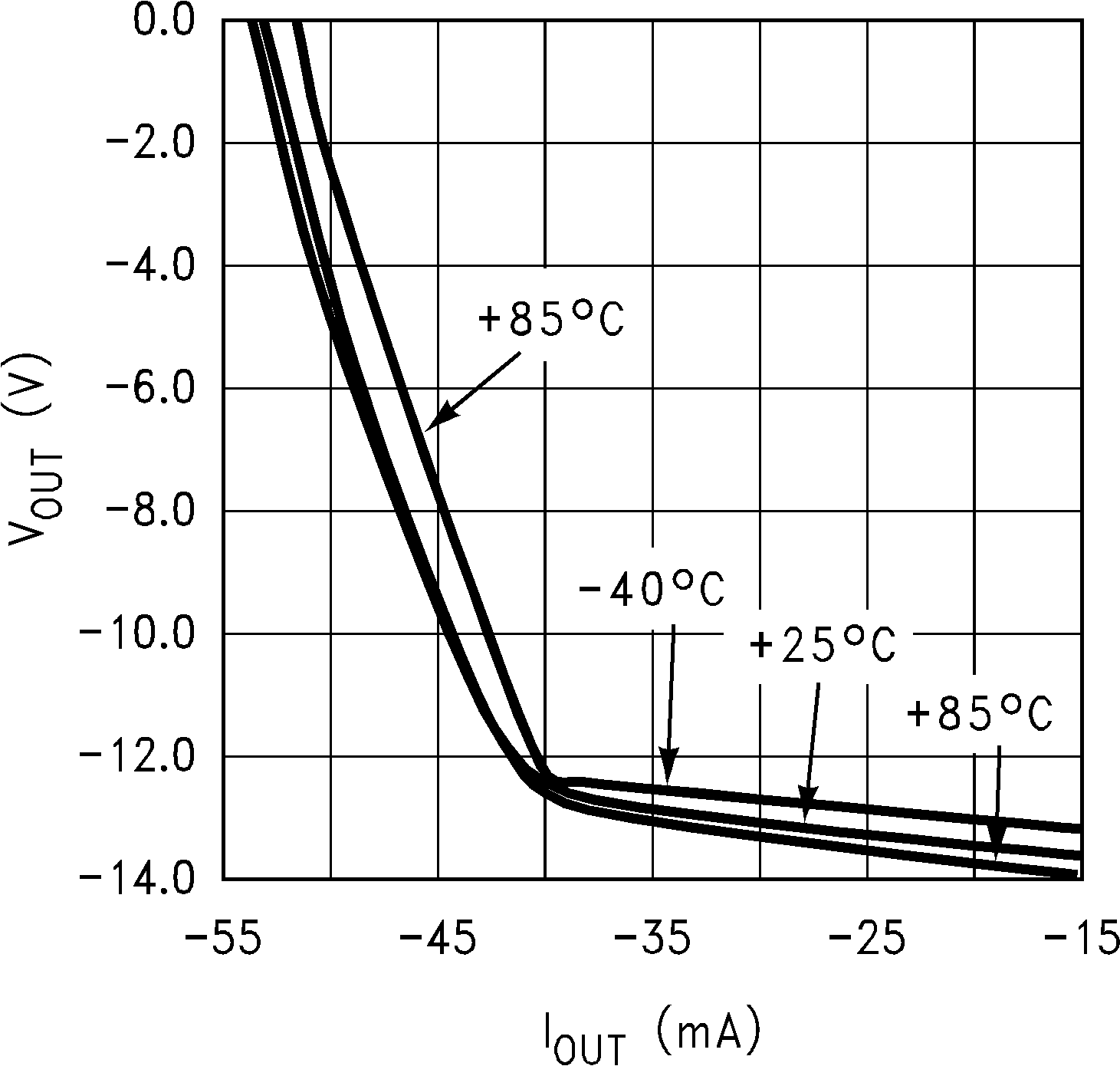
(ISINK, VS = ±15 V)
(ISOURCE, VS = ±5 V)
(ISOURCE, VS = +5 V)
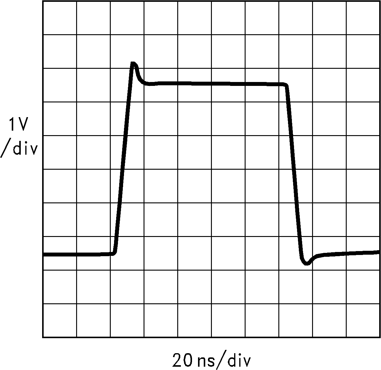
AV = -1 VS = ±15 V
AV = -1, VS = +5 V
AV = +1, VS = ±5 V
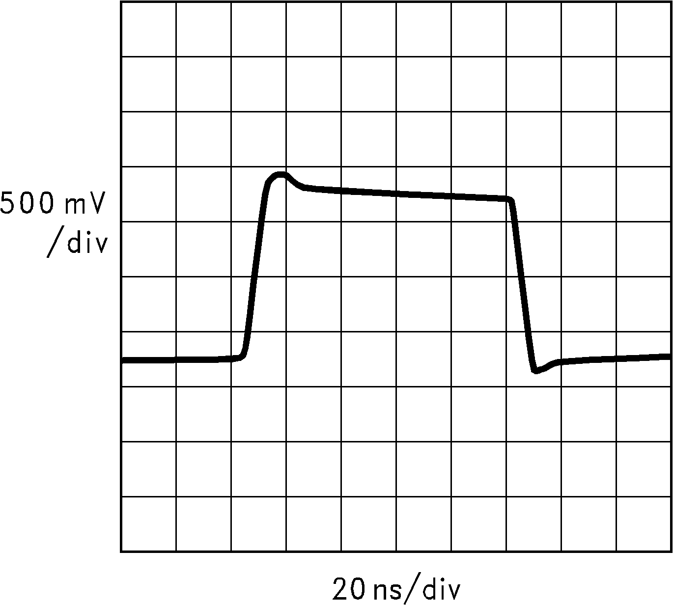
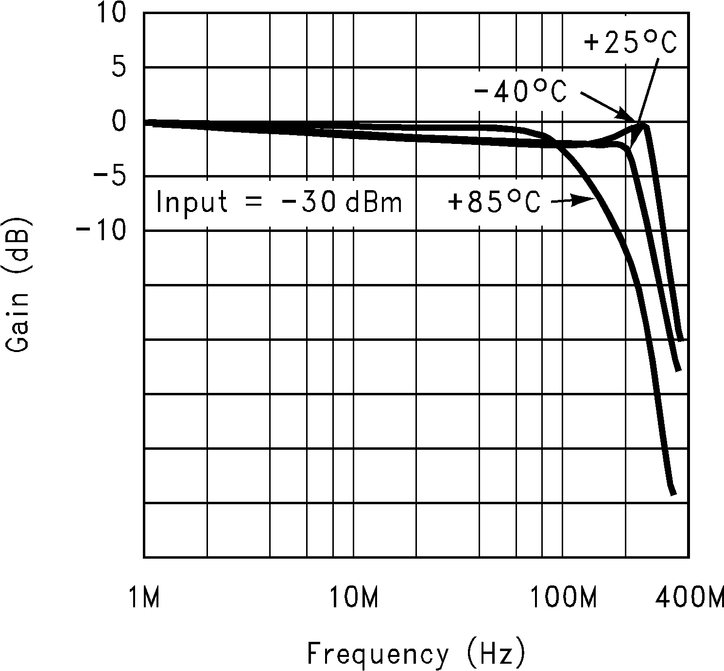
AV = +2, VS = ±15 V
AV = +2, VS = +5 V
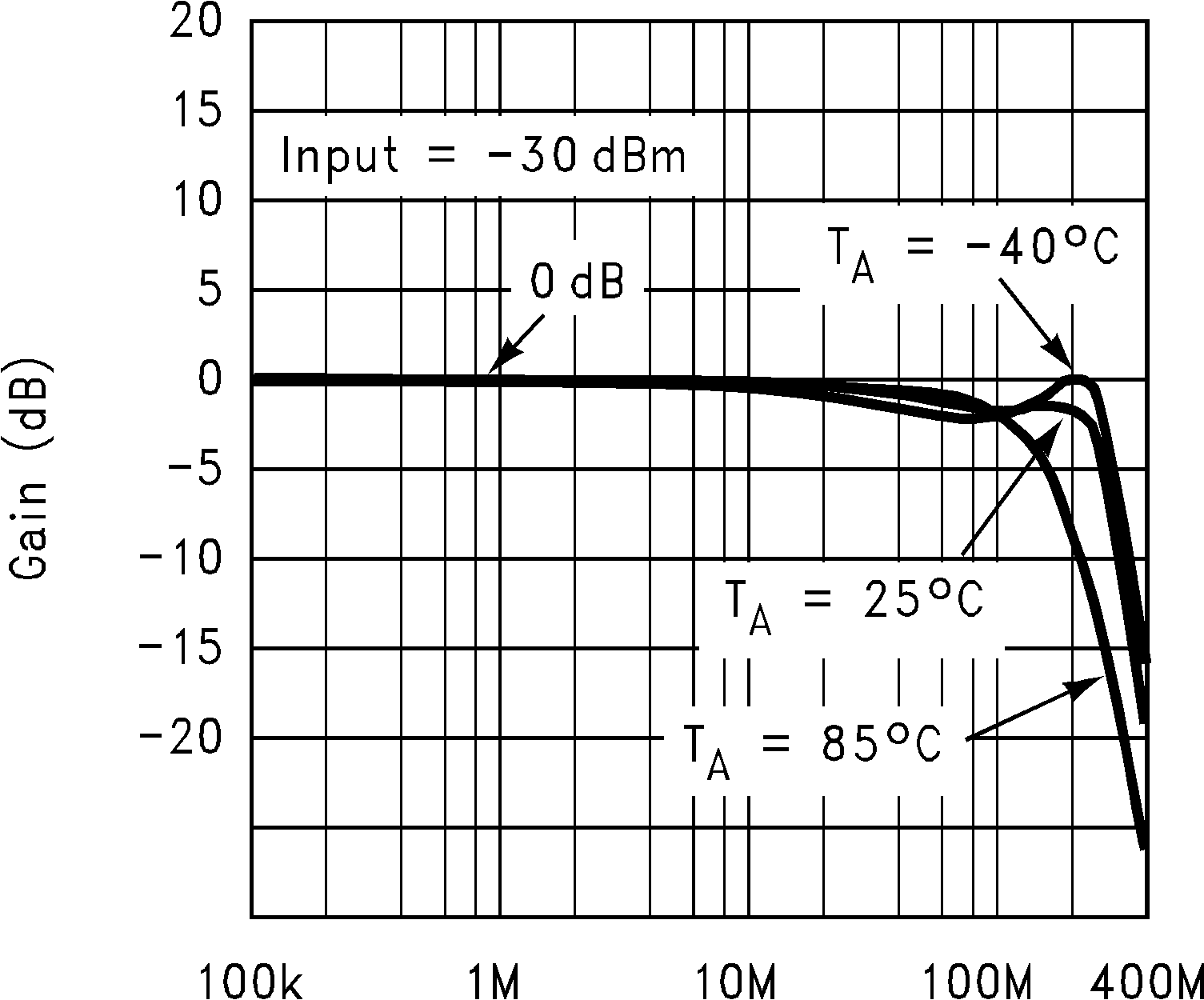
AV = - 1, VS = ±5 V, RL= 100 Ω
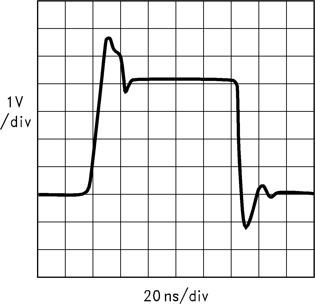
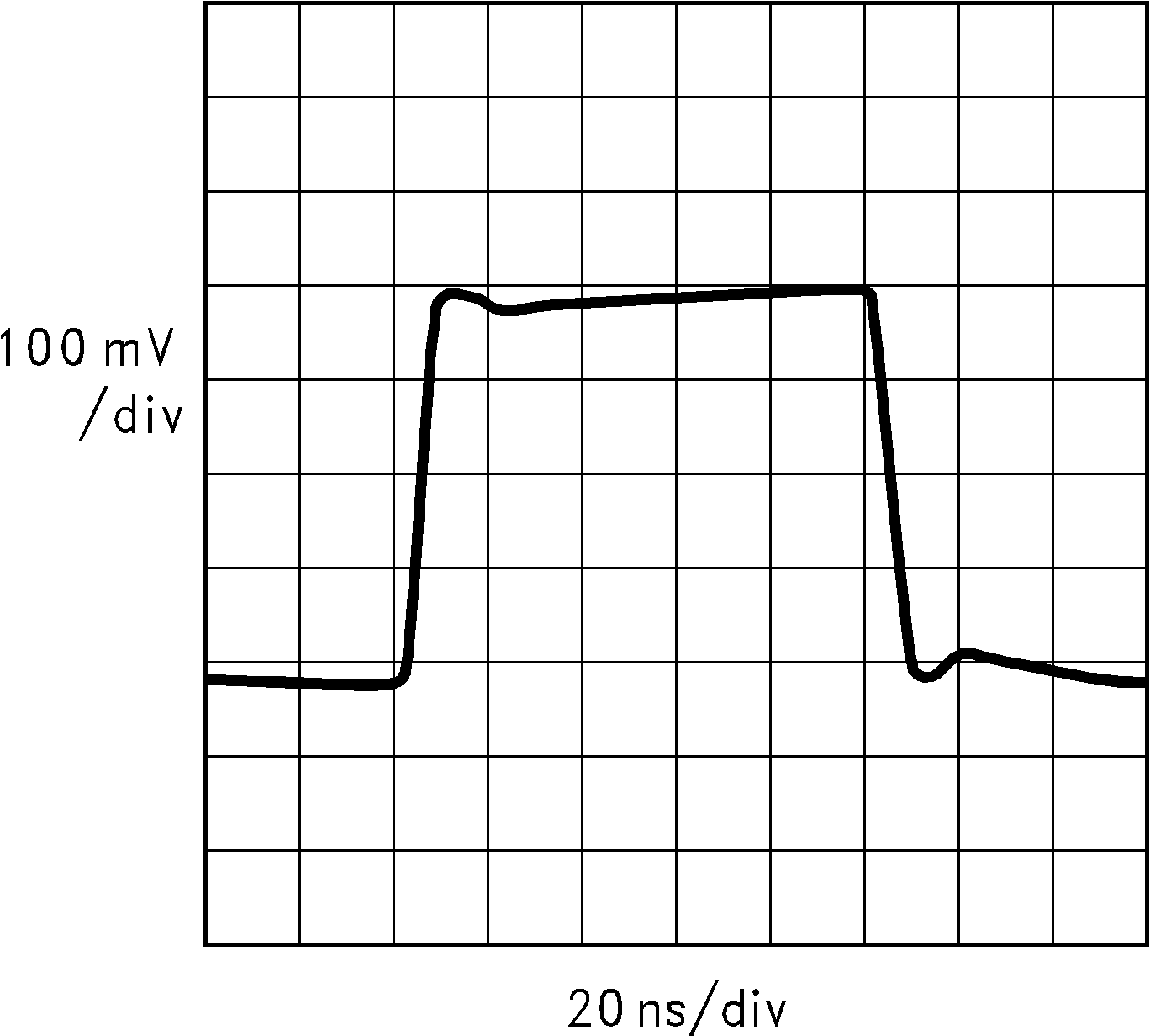
A V = +1, VS = ±15 V, RL = 100 Ω
AV = +1, VS = +5 V, RL = 100 Ω
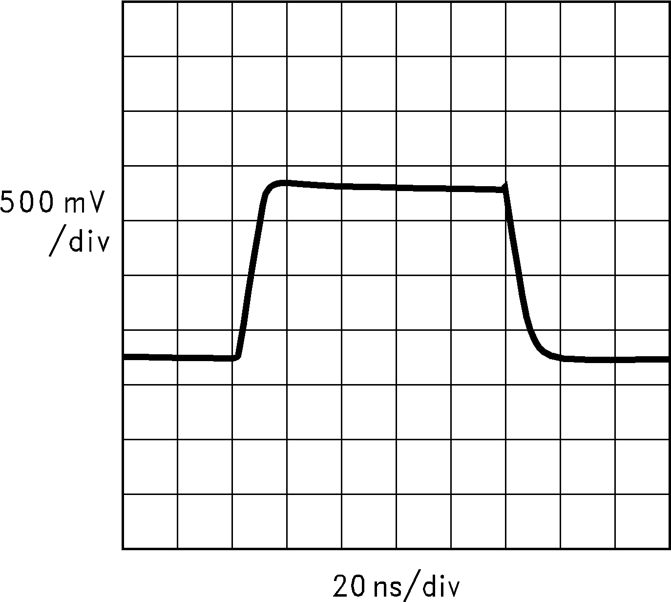
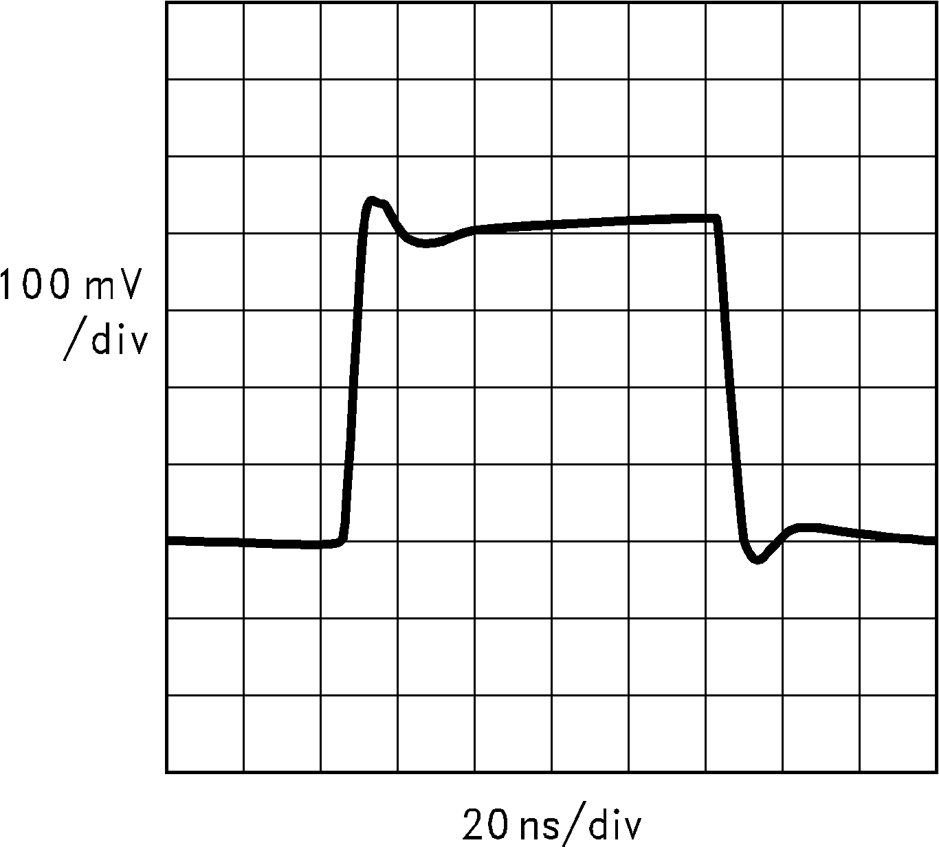
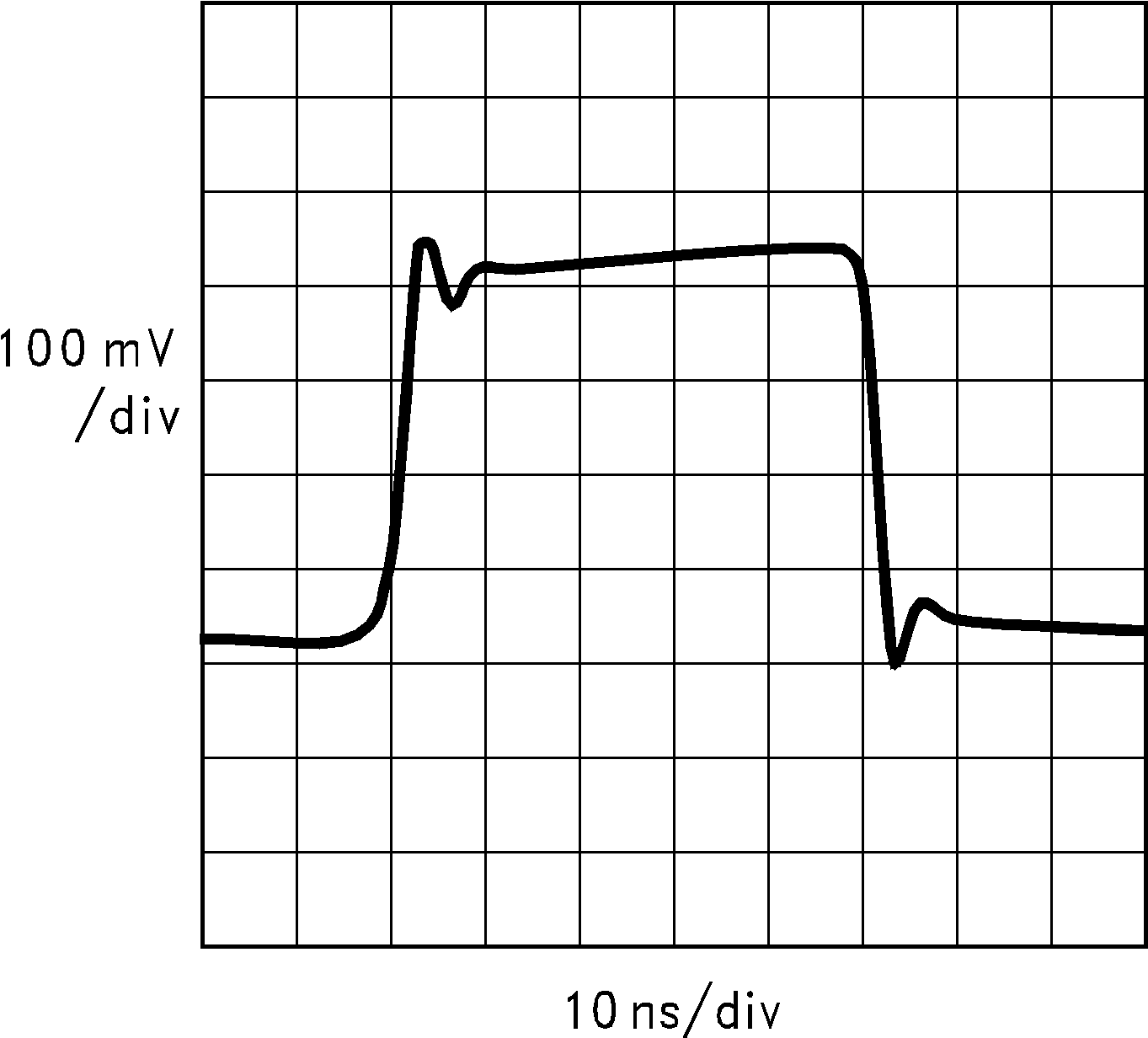
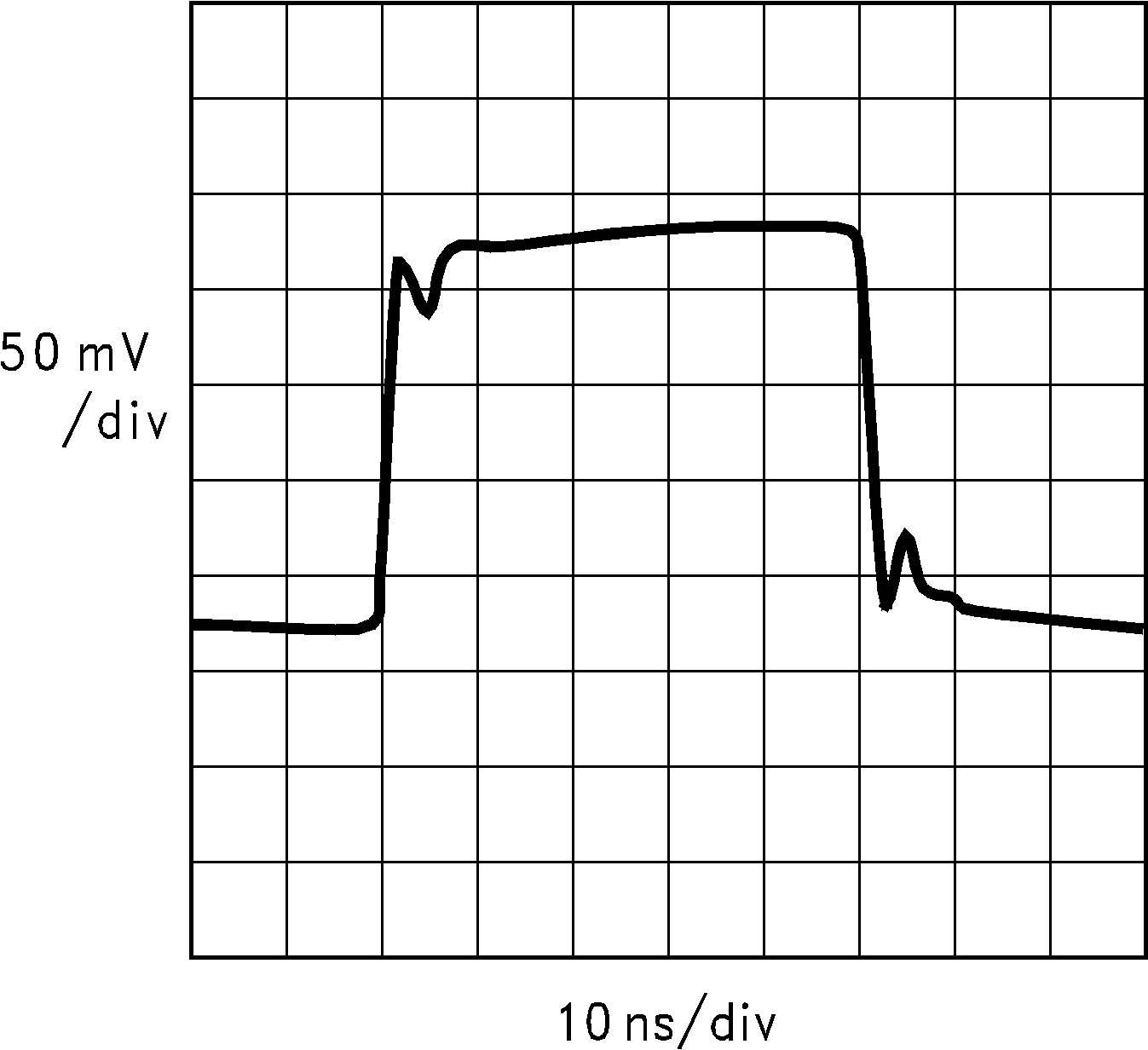
AV = +2, VS = ±5 V, RL = 100 Ω
VS = ±15 V, AV = +1, RL = 100 Ω
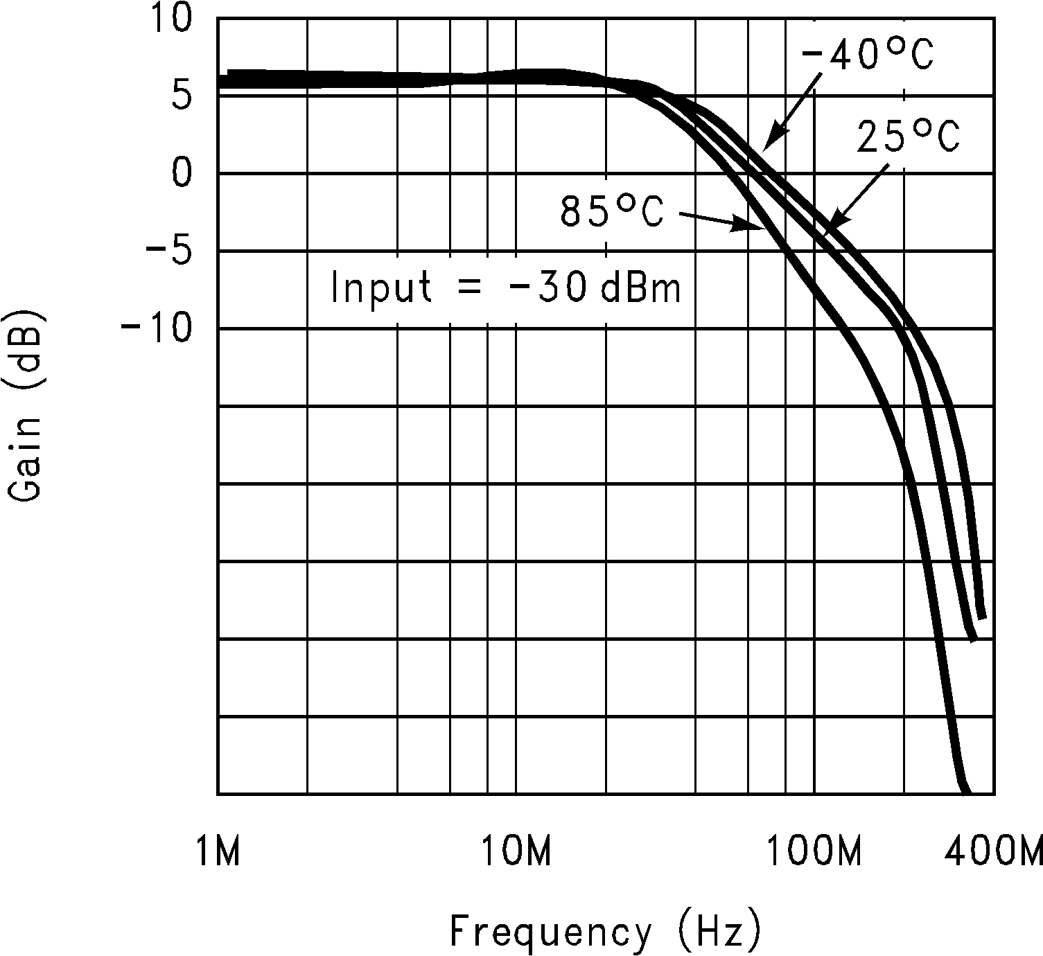
vs. Temperature,
VS = +5 V, AV = +1, RL= 100 Ω
vs. Temperature,
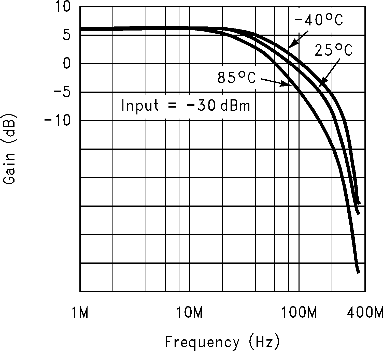
VS = ±5 V, AV = +2 , RL = 100 Ω
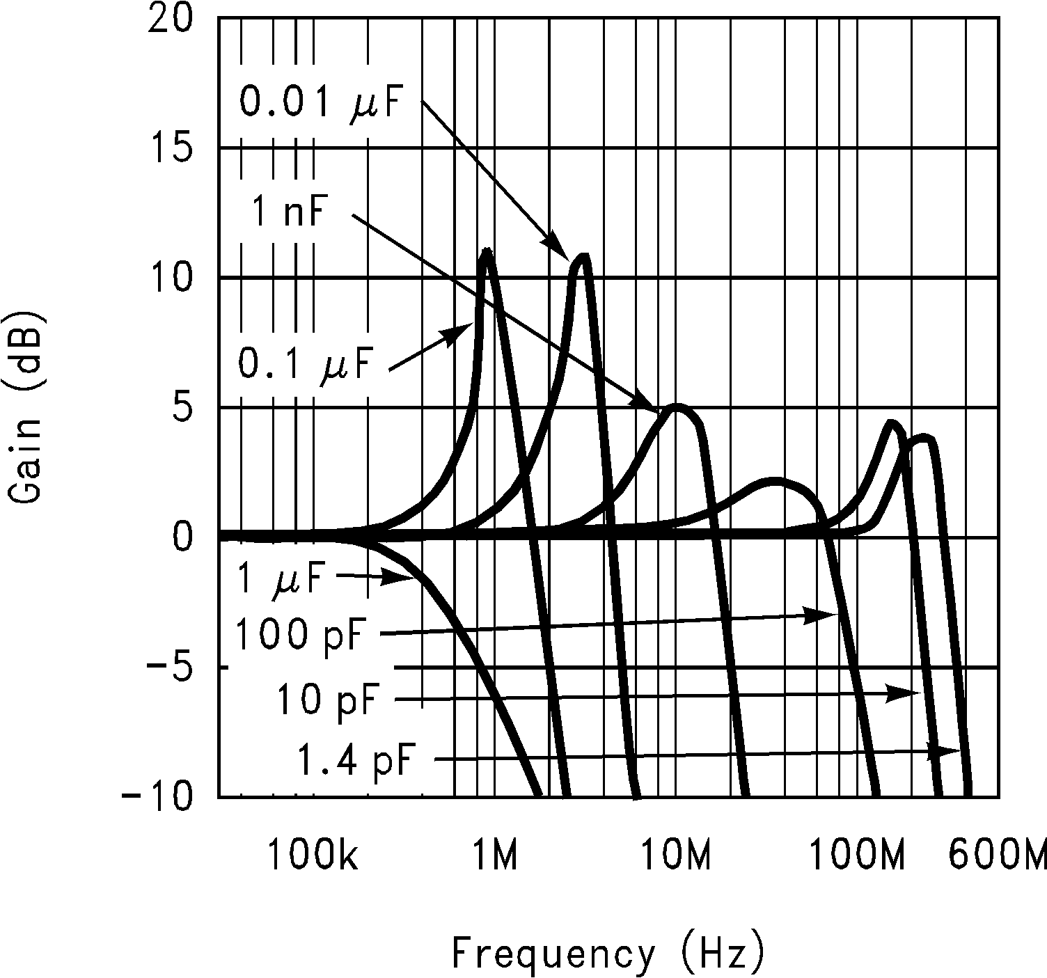
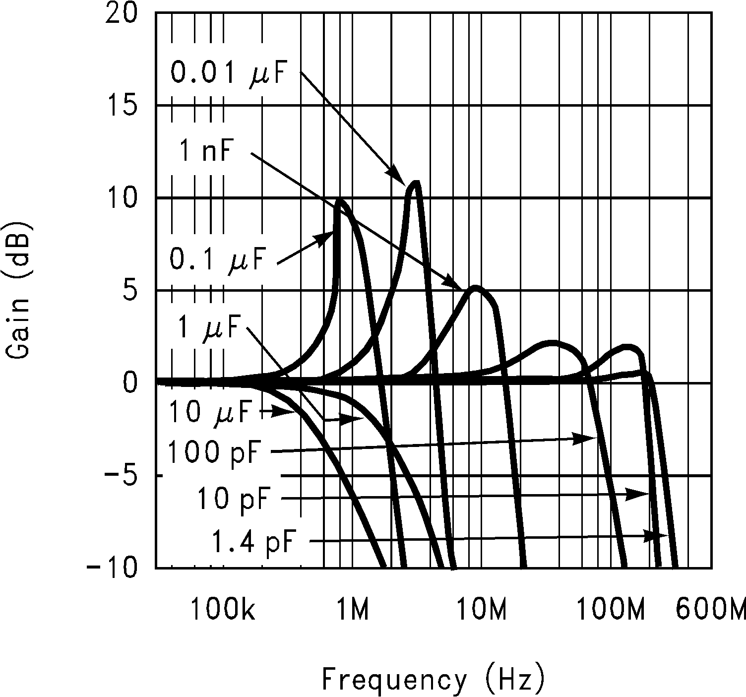
vs. Capacitance Load
(AV = +1, VS = ±15 V)
vs. Capacitive Load
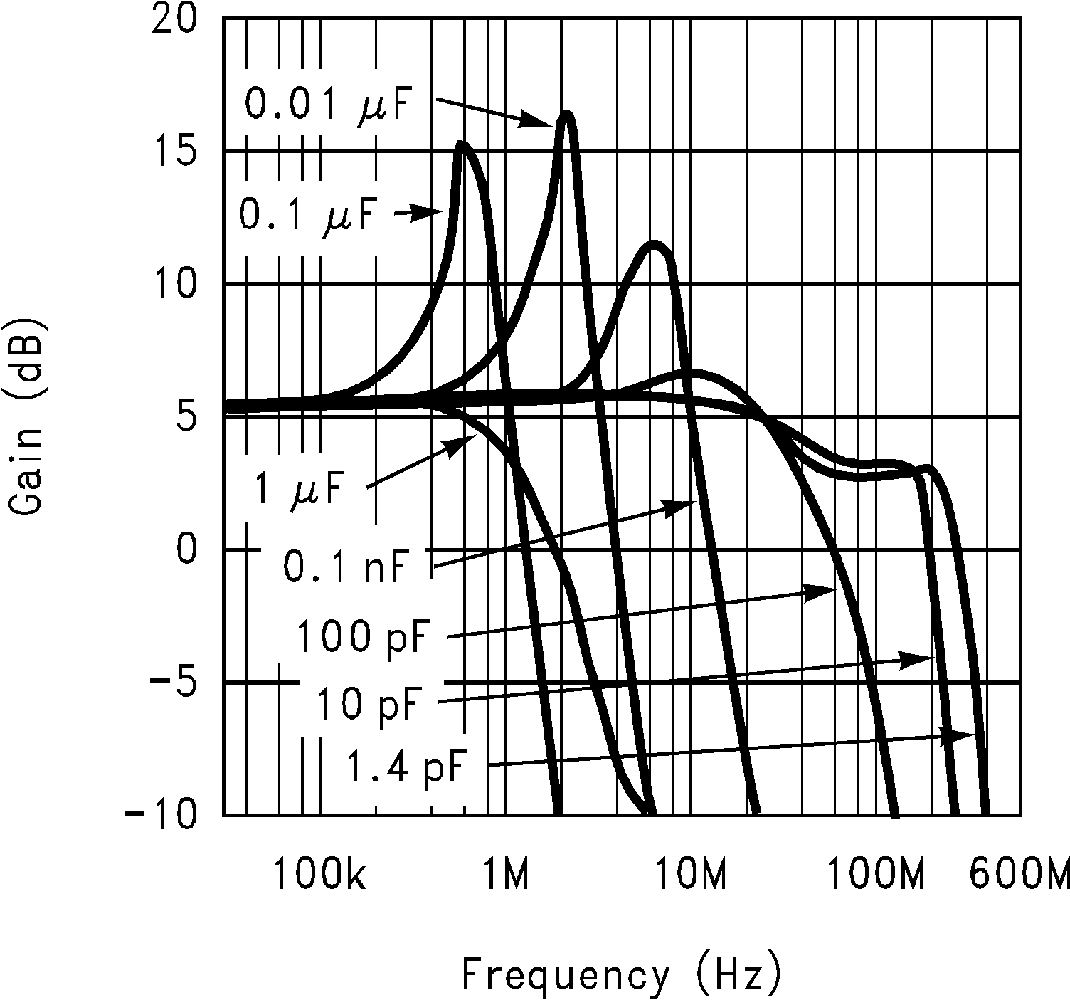
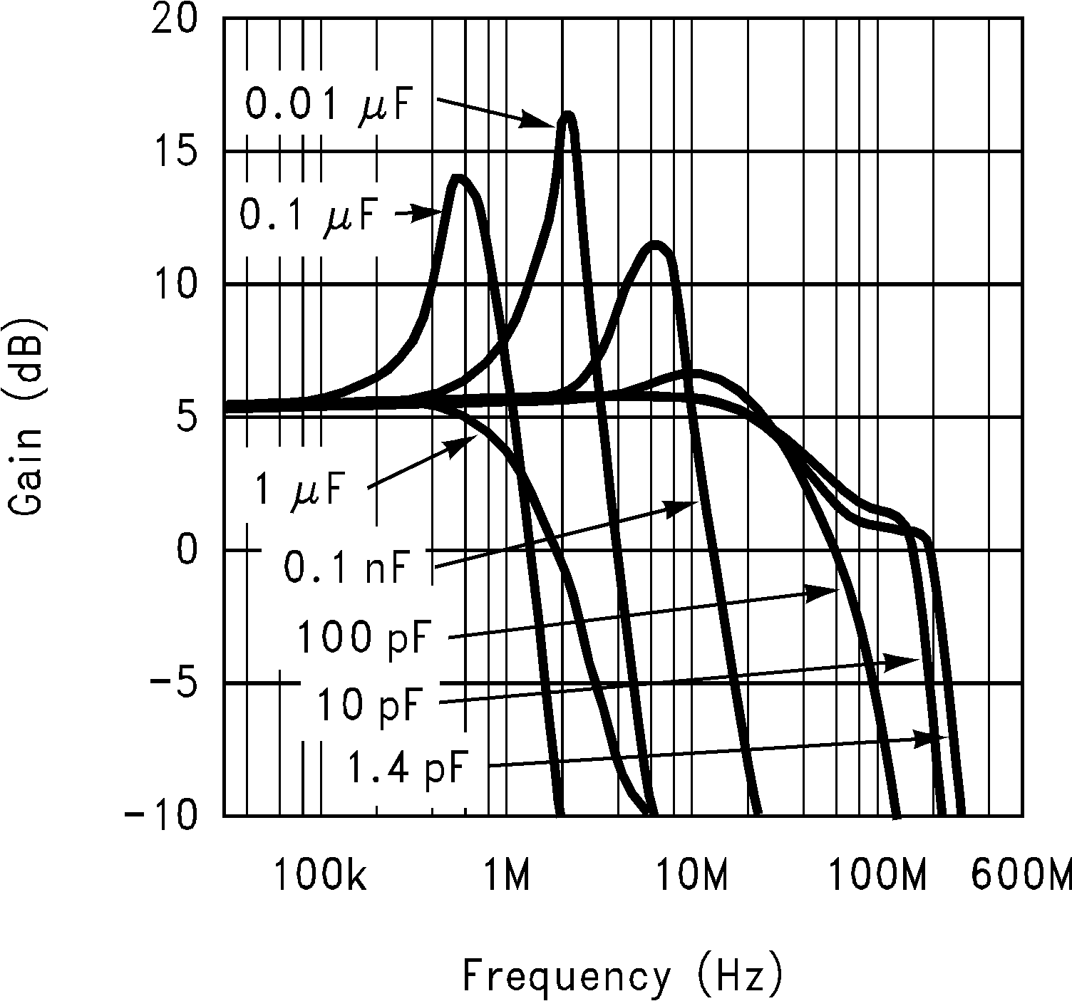
(AV = +2, VS = ±15 V)
at VS = ±5 V
(ISOURCE, VS = ±15 V)
(ISINK, VS = ±5 V)
(ISINK, VS = +5 V)
AV = -1, VS = ±5V
AV = +1, VS = ±15 V
AV = +1, VS = +5 V
AV= +2, VS = ±5 V
AV = -1, VS = ±15 V, RL = 100 Ω
AV = -1, VS = +5 V, RL = 100 Ω
A V = +1, V S = ±5 V, RL = 100 Ω

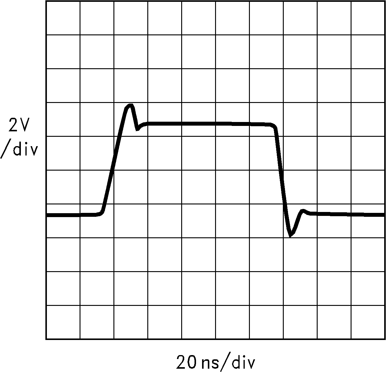
AV = +2, VS = ±15 V, RL = 100 Ω
AV = +2, VS = +5 V, RL = 100 Ω
vs. Temperature
VS = ±5 V, AV = +1, RL = 100 Ω
vs. Temperature,
VS = ±15 V, AV = +2, RL= 100 Ω
vs. Temperature,
VS = +5 V, AV = +2, RL = 100 Ω
vs. Capacitive Load
(AV = +1, VS = ±5 V)
vs. Capacitive Load
(AV = +2, VS = ±5 V)