SNVSAX6 June 2017 LM78M05-MIL
PRODUCTION DATA.
- 1 Features
- 2 Applications
- 3 Description
- 4 Revision History
- 5 Pin Configuration and Functions
- 6 Specifications
- 7 Detailed Description
- 8 Application and Implementation
- 9 Power Supply Recommendations
- 10Layout
- 11Device and Documentation Support
- 12Mechanical, Packaging, and Orderable Information
Package Options
Mechanical Data (Package|Pins)
- NDT|3
Thermal pad, mechanical data (Package|Pins)
Orderable Information
6 Specifications
6.1 Absolute Maximum Ratings
over operating free-air temperature range (unless otherwise noted)(1)(2)| MIN | MAX | UNIT | ||
|---|---|---|---|---|
| Input voltage | 5 V ≤ VO ≤ 15 V | 35 | V | |
| Power dissipation | Internally limited | |||
| Lead temperature (Soldering, 10 s) | TO package (NDT) | 300 | °C | |
| TO-220 package (NDE) | 260 | |||
| Operating junction temperature | –40 | 125 | °C | |
| Storage temperature, Tstg | –65 | 150 | °C | |
(1) Stresses beyond those listed under Absolute Maximum Ratings may cause permanent damage to the device. These are stress ratings only, which do not imply functional operation of the device at these or any other conditions beyond those indicated under Recommended Operating Conditions. Exposure to absolute-maximum-rated conditions for extended periods may affect device reliability.
(2) If Military/Aerospace specified devices are required, please contact the Texas Instruments Sales Office/Distributors for availability and specifications.
6.2 Recommended Operating Conditions
over operating free-air temperature range (unless otherwise noted)| MIN | MAX | UNIT | |
|---|---|---|---|
| Input voltage | VOUT + 1.8 | 35 | V |
| Output current | 0.5 | A |
6.3 Thermal Information
| THERMAL METRIC(1) | LM78M05 | UNIT | ||
|---|---|---|---|---|
| NDP (TO-252) |
NDT (TO) |
|||
| 3 PINS | 3 PINS | |||
| RθJA | Junction-to-ambient thermal resistance | 38 | 162.4 | °C/W |
| RθJC(top) | Junction-to-case (top) thermal resistance | 48.4 | 23.9 | °C/W |
| RθJB | Junction-to-board thermal resistance | 17.7 | — | °C/W |
| ψJT | Junction-to-top characterization parameter | 6.7 | — | °C/W |
| ψJB | Junction-to-board characterization parameter | 17.9 | — | °C/W |
| RθJC(bot) | Junction-to-case (bottom) thermal resistance | 4.4 | — | °C/W |
(1) For more information about traditional and new thermal metrics, see the Semiconductor and IC Package Thermal Metrics application report.
6.4 Electrical Characteristics
VIN = 10 V, CIN = 0.33 µF, CO = 0.1 µF, TJ = 25°C (unless otherwise noted). Limits are specified by production testing or correlation techniques using standard Statistical Quality Control (SQC) methods.| PARAMETER | TEST CONDITIONS | MIN | TYP | MAX | UNIT | ||
|---|---|---|---|---|---|---|---|
| VO | Output voltage | IL = 500 mA | 4.8 | 5 | 5.2 | V | |
| 5 mA ≤ IL ≤ 500 mA, PD ≤ 7.5 W, 7.5 V ≤ VIN ≤ 20 V, –40°C ≤ TJ ≤ 125°C |
4.75 | 5 | 5.25 | ||||
| VRLINE | Line regulation | 7.2 V ≤ VIN ≤ 25 V | IL = 100 mA | 50 | mV | ||
| IL = 500 mA | 100 | ||||||
| VRLOAD | Load regulation | IL = 5 mA to 500 mA | 100 | mV | |||
| IQ | Quiescent current | IL = 500 mA | 4 | 10 | mA | ||
| ΔIQ | Quiescent current change | 5 mA ≤ IL ≤ 500 mA, | 0.5 | mA | |||
| 7.5 V ≤ VIN ≤ 25 V, IL = 500 mA | 1 | ||||||
| Vn | Output noise voltage | 10 Hz ≤ f ≤ 100 kHz | 40 | µV | |||
| ΔVIN | Ripple rejection | f = 120 Hz, IL = 500 mA | 78 | dB | |||
| VIN | Input voltage required to maintain line regulation | IL = 500 mA | 7.2 | V | |||
| ΔVO | Long-term stability | IL = 500 mA, –40°C ≤ TJ ≤ 125°C | 20 | mV/khrs | |||
6.5 Typical Characteristics
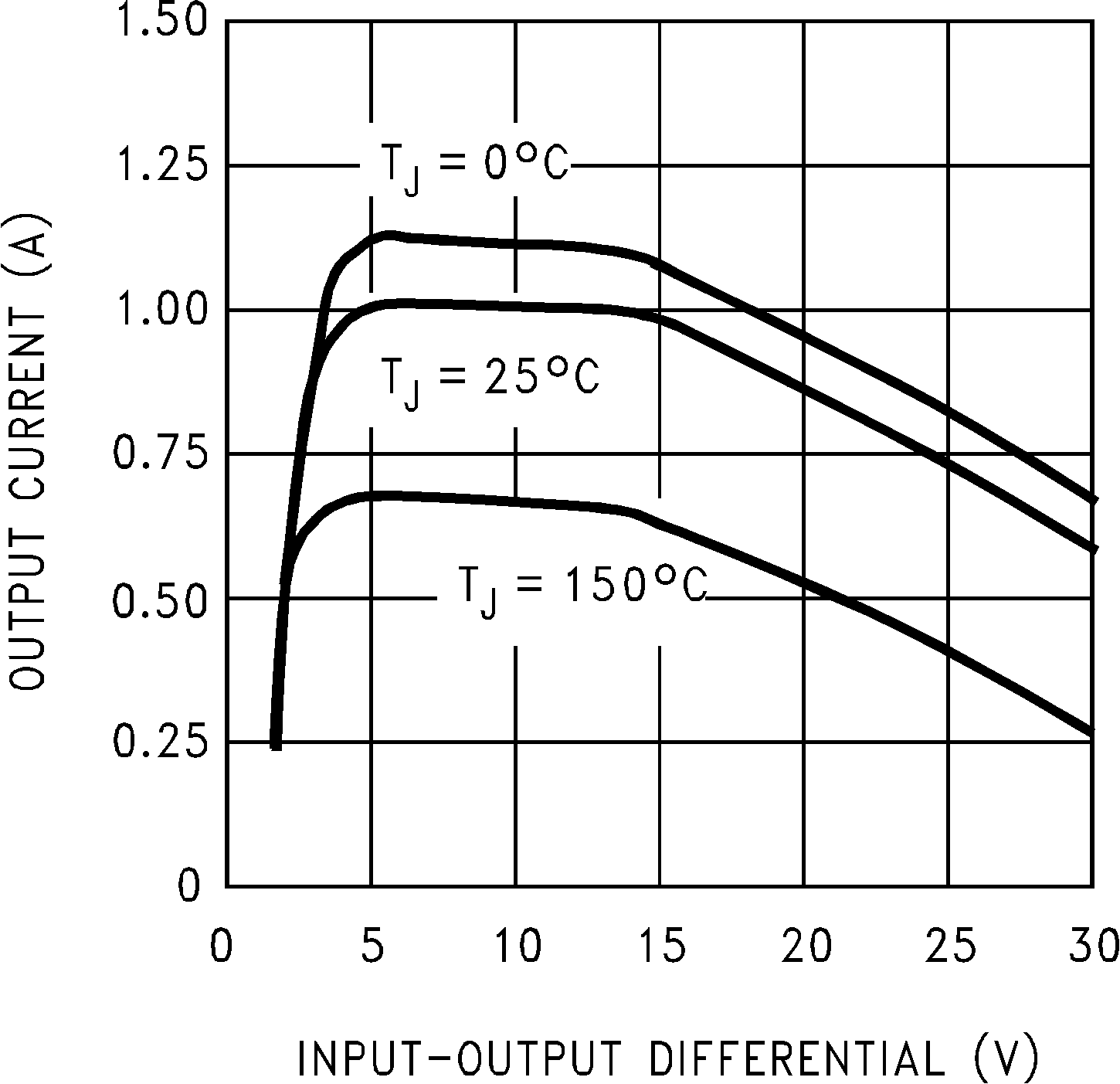 Figure 1. Peak Output Current
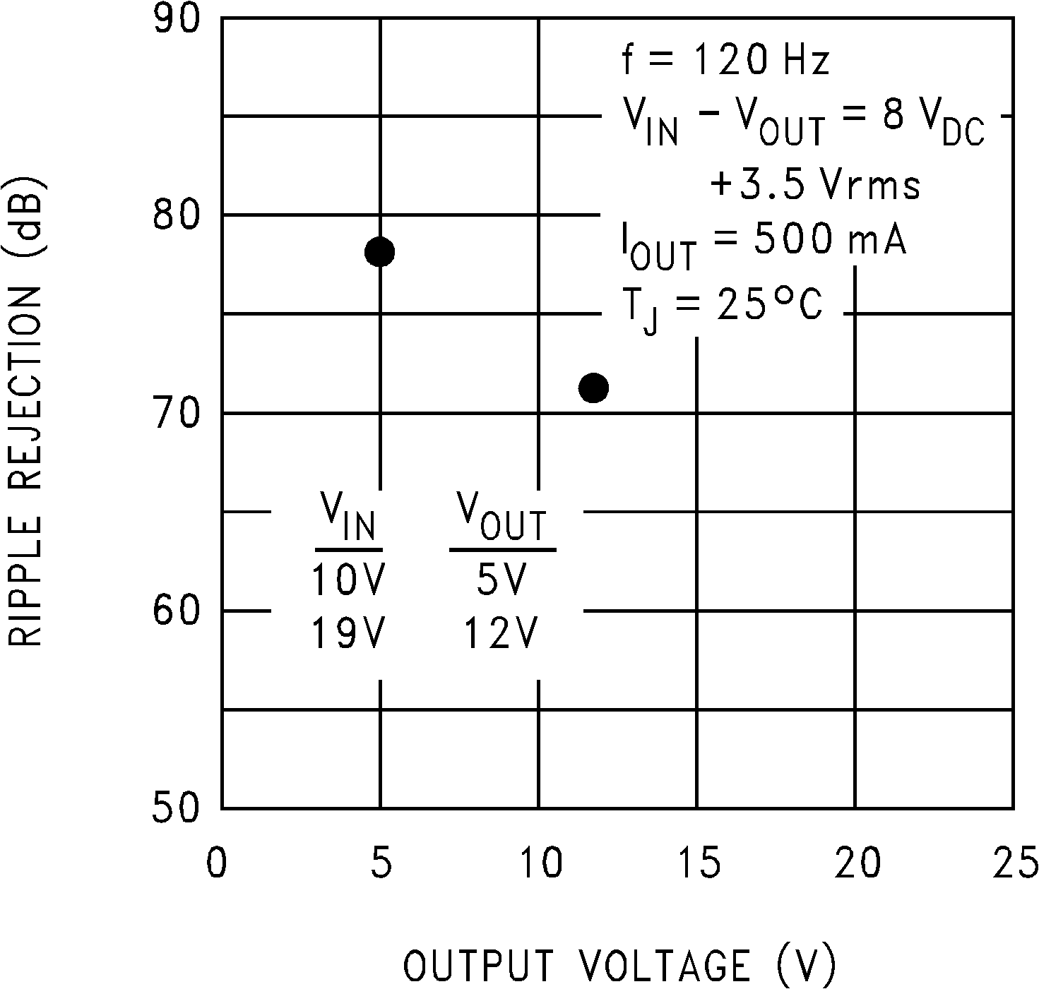 Figure 3. Ripple Rejection
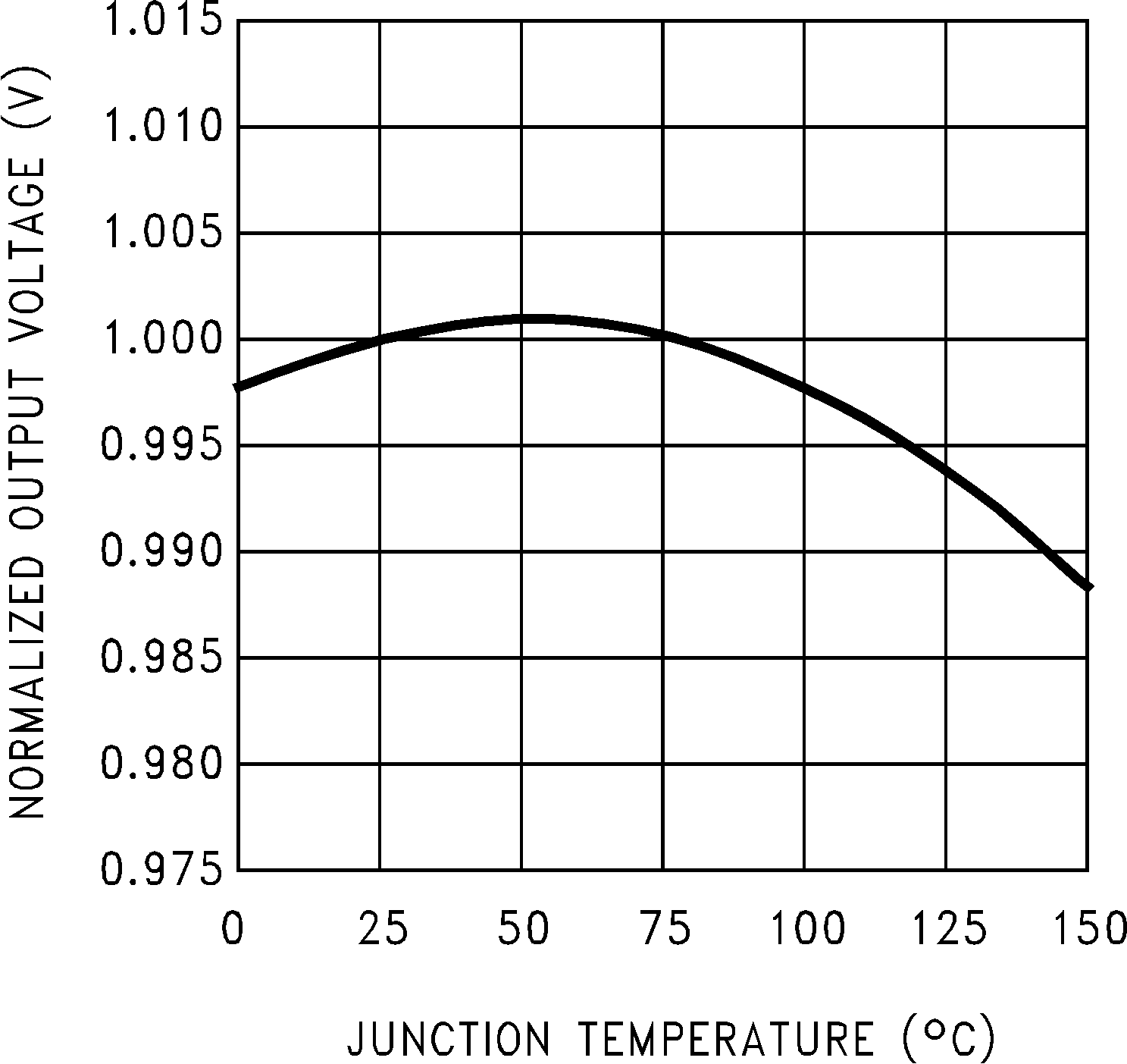
| Normalized to 1 V | TJ = 25°C |
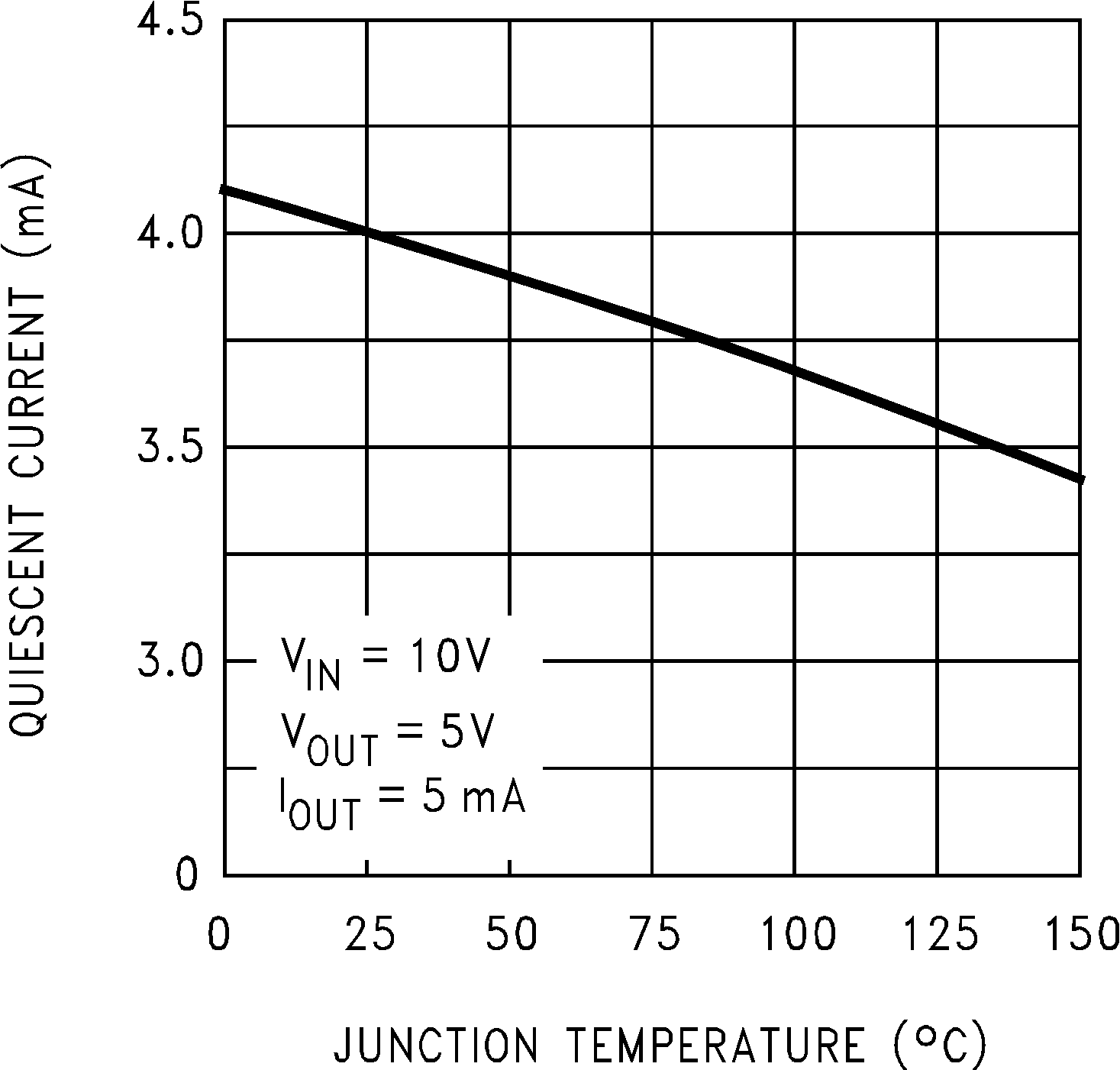 Figure 7. Quiescent Current
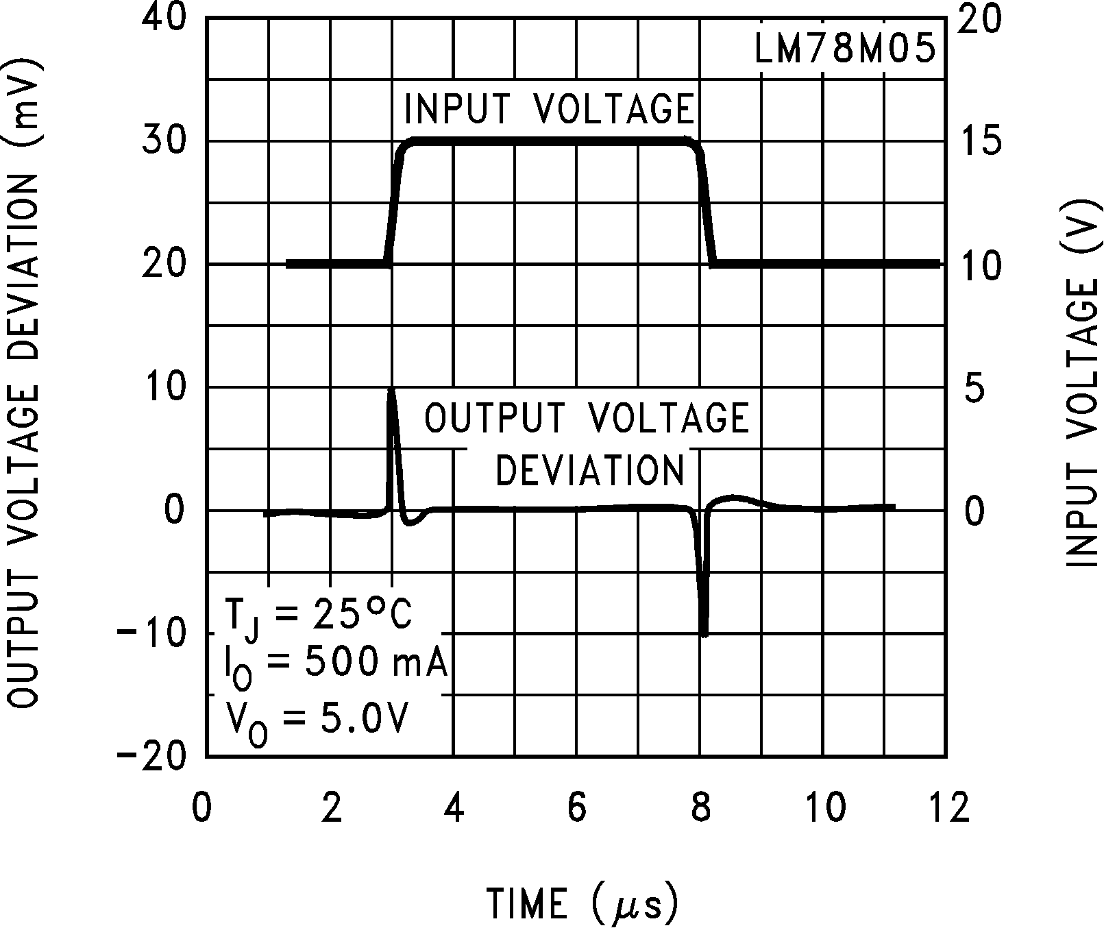 Figure 9. Line Transient Response
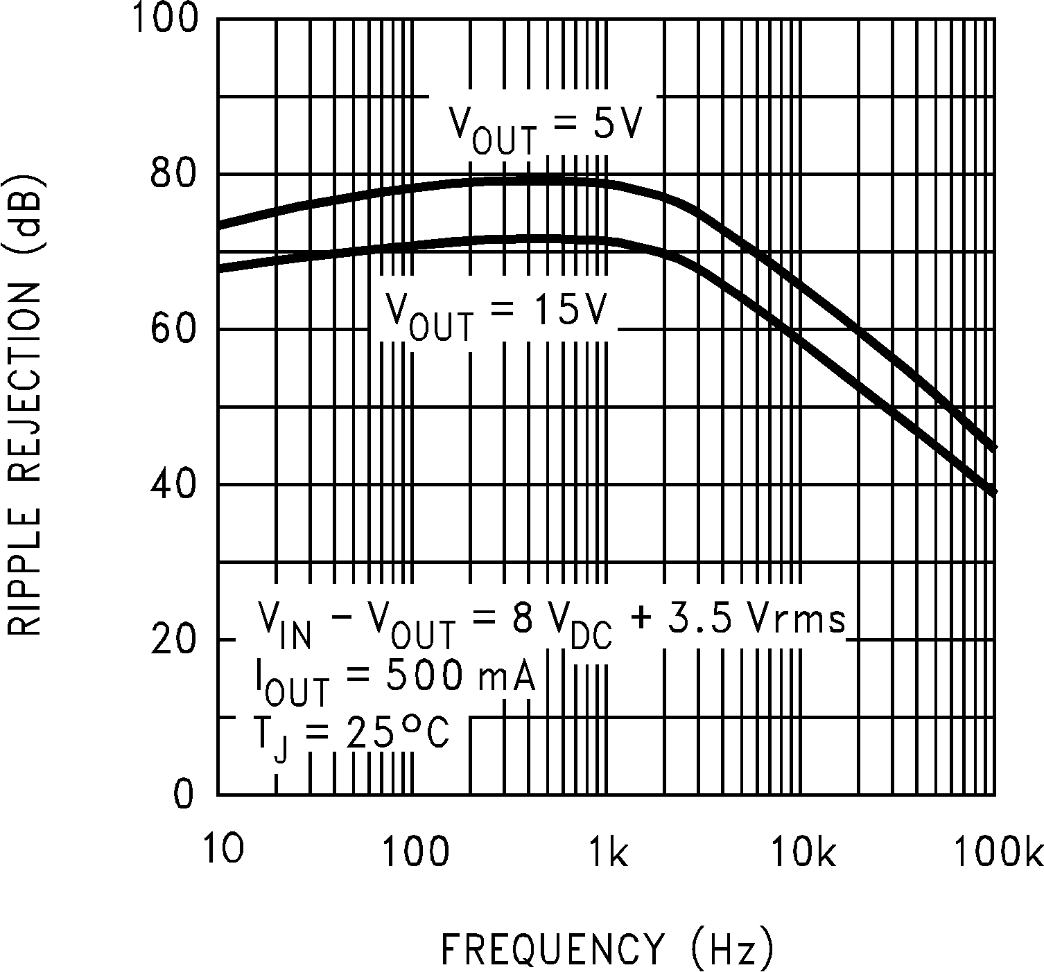 Figure 2. Ripple Rejection
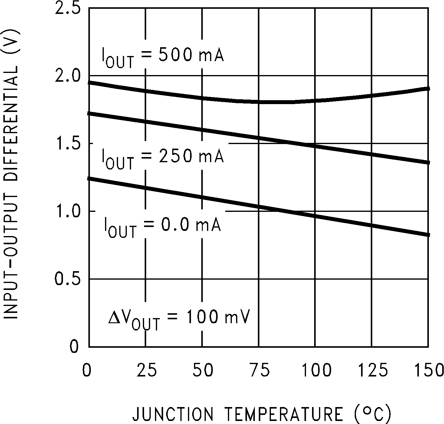 Figure 4. Dropout Voltage
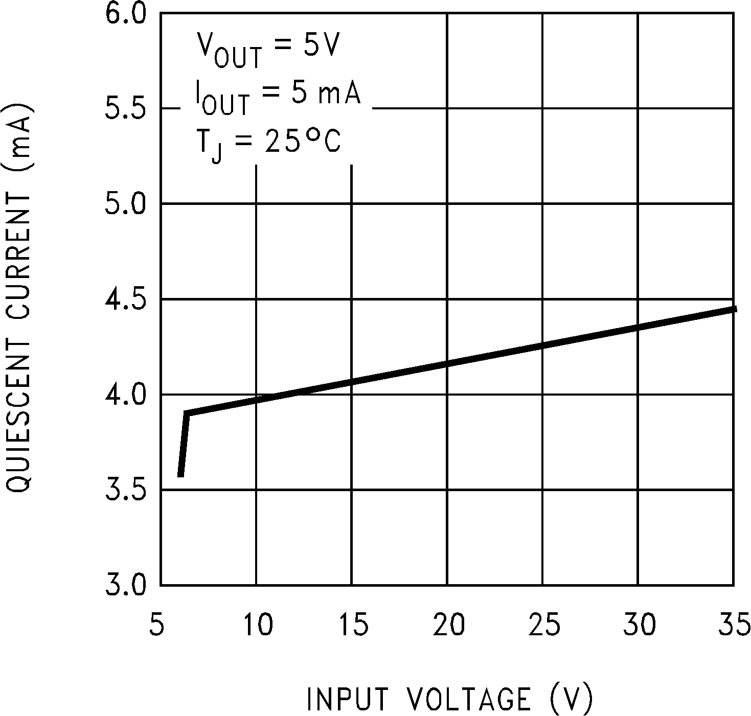
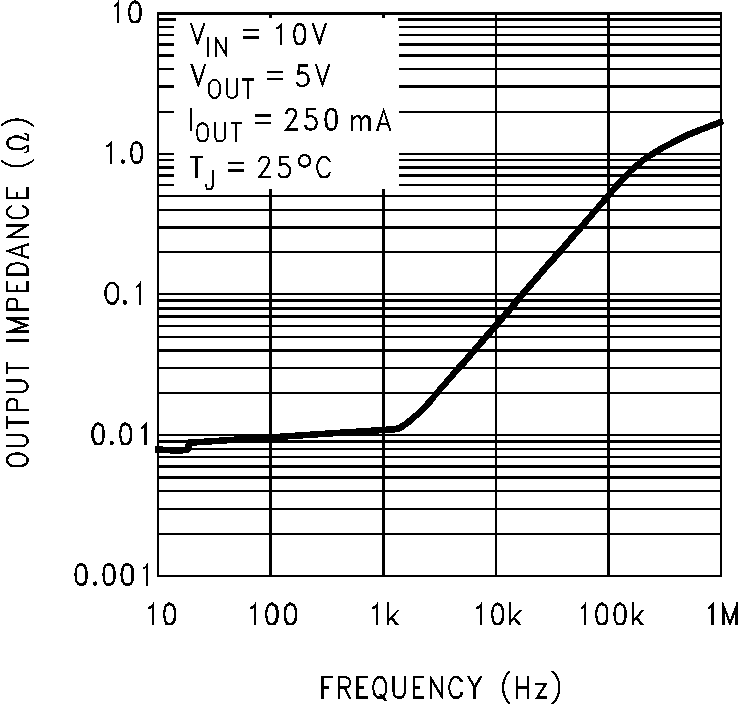 Figure 8. Output Impedance
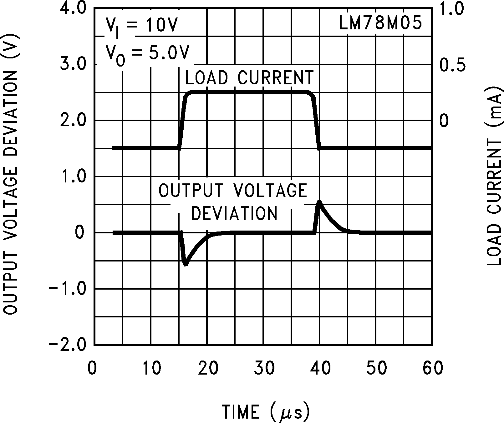 Figure 10. Load Transient Response