SNIS146B March 2007 – October 2017 LM95214
PRODUCTION DATA.
- 1 Features
- 2 Applications
- 3 Description
- 4 Revision History
- 5 Pin Configuration and Functions
-
6 Specifications
- 6.1 Absolute Maximum Ratings
- 6.2 ESD Ratings
- 6.3 Recommended Operating Conditions
- 6.4 Thermal Information
- 6.5 Electrical Characteristics: Temperature-to-Digital Converter
- 6.6 Logic Electrical Characteristics: Digital DC Characteristics
- 6.7 Switching Characteristics: SMBus Digital
- 6.8 Typical Characteristics
-
7 Detailed Description
- 7.1 Overview
- 7.2 Functional Block Diagram
- 7.3 Feature Description
- 7.4 Device Functional Modes
- 7.5 Register Maps
- 8 Application and Implementation
- 9 Power Supply Recommendations
- 10Layout
- 11Device and Documentation Support
- 12Mechanical, Packaging, and Orderable Information
Package Options
Mechanical Data (Package|Pins)
- NHL|14
Thermal pad, mechanical data (Package|Pins)
Orderable Information
7 Detailed Description
7.1 Overview
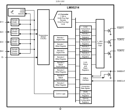
The LM95214 is an 11-bit digital temperature sensor with a 2-wire System Management Bus (SMBus) interface that can monitor the temperature of four remote diodes as well as its own temperature. The LM95214 can be used to very accurately monitor the temperature of up to four external devices such as microprocessors, graphics processors or diode-connected 2N3904 transistor. Any device whose thermal diode can be modeled by an MMBT3904 transistor will work well with the LM95214.
The LM95214 reports temperature in two different formats for +127.875°C/–128°C range and 0°C/255°C range. The LM95214 has a Sigma-Delta ADC (Analog-to-Digital Converter) core which provides the first level of noise immunity. For improved performance in a noisy environment the LM95214 includes programmable digital filters for Remote Diode 1 and 2 temperature readings. When the digital filters are invoked the resolution for Remote Diode 1 and 2 readings increases to 0.03125°C. For maximum flexibility and best accuracy the LM95214 includes offset registers that allow calibration of other diode types.
7.2 Functional Block Diagram
7.3 Feature Description
The LM95214 TCRIT1, TCRIT2, and TCRIT3 active low outputs are triggered when any unmasked channel exceeds its corresponding programmable limit and can be used to shutdown the system, to turn on the system fans or as a microcontroller interrupt function. The current status of the TCRIT1, TCRIT2, and TCRIT3 pins can be read back from the status registers through the SMBus interface. Two of the remote channels have two separate limits each that control the TCRIT1 and TCRIT2 pins. The remaining two channels and the local channel each have one limit to control both the TCRIT1 and TCRIT2 pins. The TCRIT3 pin shares the limits of the TCRIT2 pin but allows for different masking options. All limits have a shared programmable hysteresis register.
Diode fault detection circuitry in the LM95214 can detect the absence or fault state of a remote diode: whether D+ is shorted to VDD, D– or ground, or whether D+ is floating.
Remote Diode 1 and 2 temperature channels have programmable digital filters while the other two remote temperature channels utilize a fault-queue to avoid false triggering the TCRIT pins.
The LM95214 has a three-level address pin to connect up to 3 devices to the same SMBus master. LM95214 also has programmable conversion rate register as well as a shutdown mode for power savings. One round of conversions can be triggered in shutdown mode by writing to the one-shot register through the SMBus interface. LM95214 can be programmed to turn off unused channels for more power savings.
The LM95214 register set has an 8-bit data structure and includes:
- Temperature Value Registers with signed format
- Most-Significant-Byte (MSB) and Least-Significant-Byte (LSB) Local Temperature
- MSB and LSB Remote Temperature 1
- MSB and LSB Remote Temperature 2
- MSB and LSB Remote Temperature 3
- MSB and LSB Remote Temperature 4
- Temperature Value Registers with unsigned format
- MSB and LSB Remote Temperature 1
- MSB and LSB Remote Temperature 2
- MSB and LSB Remote Temperature 3
- MSB and LSB Remote Temperature 4
- Diode Configuration Registers
- Diode Model Select
- Remote 1 Offset
- Remote 2 Offset
- Remote 3 Offset
- Remote 4 Offset
- General Configuration Registers
- Configuration (Standby, Fault Queue enable for Remote 3 and 4; Conversion Rate)
- Channel Conversion Enable
- Filter Setting for Remote 1 and 2
- 1-Shot
- Status Registers
- Main Status Register (Busy bit, Not Ready, Status Register 1 to 4 Flags)
- Status 1 (diode fault)
- Status 2 (TCRIT1)
- Status 3 (TCRIT2)
- Status 4 (TCRIT3)
- Mask Registers
- TCRIT1 Mask
- TCRIT2 Mask
- TCRIT3 Mask
- Limit Registers
- Local Tcrit Limit
- Remote 1 Tcrit-1 Limit
- Remote 2 Tcrit-1 Limit
- Remote 3 Tcrit Limit
- Remote 4 Tcrit Limit
- Remote 1 Tcrit-2 and Tcrit-3 Limit
- Remote 2 Tcrit-2 and Tcrit-3 Limit
- Common Tcrit Hysteresis
- Manufacturer ID Register
- Revision ID Register
7.3.1 Conversion Sequence
The LM95214 takes approximately 190 ms to convert the Local Temperature, Remote Temperatures 1 through 4, and to update all of its registers. These conversions for each thermal diode are addressed in a round robin sequence. Only during the conversion process the busy bit (D7) in Status register (02h) is high. The conversion rate may be modified by the Conversion Rate bits found in the Configuration Register (03h). When the conversion rate is modified a delay is inserted between each round of conversions, the actual time for each round remains at 190 ms (typical all channels enabled). The time a round takes depends on the number of channels that are on. Different conversion rates will cause the LM95214 to draw different amounts of average supply current as shown in Figure 10. This curve assumes all the channels are on. If channels are turned off the average current will drop because the round robin time will decrease and the shutdown time will increase during each conversion interval.
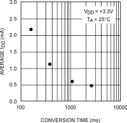 Figure 10. Conversion Rate Effect on Power Supply Current
7.3.2 Power-On-Default States
The LM95214 always powers up to these known default states. The LM95214 remains in these states until after the first conversion.
- All Temperature readings set to 0°C until the end of the first conversion
- Remote offset for all channels 0°C
- Configuration: Active converting, Fault Queue enabled for Remote 3 and 4
- Continuous conversion with all channels enabled, time = 1 s
- Enhanced digital filter enabled for Remote 1 and 2
- Status Registers depends on state of thermal diode inputs
- Local and Remote Temperature Limits for TCRIT1, TCRIT2 and TCRIT3 outputs:
- Manufacturers ID set to 01h
- Revision ID set to 79h
Table 2. Temperature Channel limits
| OUTPUT PIN | TEMPERATURE CHANNEL LIMIT | ||||
|---|---|---|---|---|---|
| REMOTE 4 (°C) |
REMOTE 3 (°C) |
REMOTE 2 (°C) |
REMOTE 1 (°C) |
LOCAL (°C) |
|
| TCRIT1 | Masked, 85 |
Masked, 85 |
110 | 110 | Masked, 85 |
| TCRIT2 | 85 | 85 | 85 | 85 | 85 |
| TCRIT3 | 85 | 85 | Masked, 85 |
Masked, 85 |
Masked, 85 |
7.3.3 SMBus Interface
The LM95214 operates as a slave on the SMBus, so the SMBCLK line is an input and the SMBDAT line is bidirectional. The LM95214 never drives the SMBCLK line and it does not support clock stretching. According to SMBus specifications, the LM95214 has a 7-bit slave address. Three SMBus device address can be selected by connecting A0 (pin 6) to either Low, Mid-Supply, or High voltages. The LM95214 has the following SMBus slave address:
Table 3. SMBus Slave Addresses
| A0 PIN STATE | SMBus DEVICE ADDRESS A[6:0] | |
|---|---|---|
| HEX | BINARY | |
| Low | 18h | 001 1000 |
| Mid-Supply | 4Dh | 100 1101 |
| High | 4Eh | 100 1110 |
7.3.4 Temperature Conversion Sequence
Each of the 5 temperature channels of LM95214 can be turned OFF independent from each other through the Channel Enable Register. Turning off unused channels will increase the conversion speed in the fastest conversion speed mode. If the slower conversion speed settings are used, disabling unused channels will reduce the average power consumption of LM95214.
7.3.4.1 Digital Filter
To suppress erroneous remote temperature readings due to noise as well as increase the resolution of the temperature, the LM95214 incorporates a digital filter for Remote 1 and 2 Temperature Channels. When a filter is enabled the filtered readings are used for the TCRIT comparisons. There are two possible digital filter settings that are enabled through the Filter Setting Register at register address 0Fh. The filter for each channel can be set according to the following table:
Table 4. Digital Filter Settings
| R1F[1:0] OR R2F[1:0] | FILTER SETTING | |
|---|---|---|
| 0 | 0 | No Filter |
| 0 | 1 | Filter (equivalent to Level 2 filter of the LM86/LM89) |
| 1 | 0 | Reserved |
| 1 | 1 | Enhanced Filter (Filter with transient noise clipping) |
Figure 11, Figure 12, and Figure 13 describe the filter output in response to a step input and an impulse input.
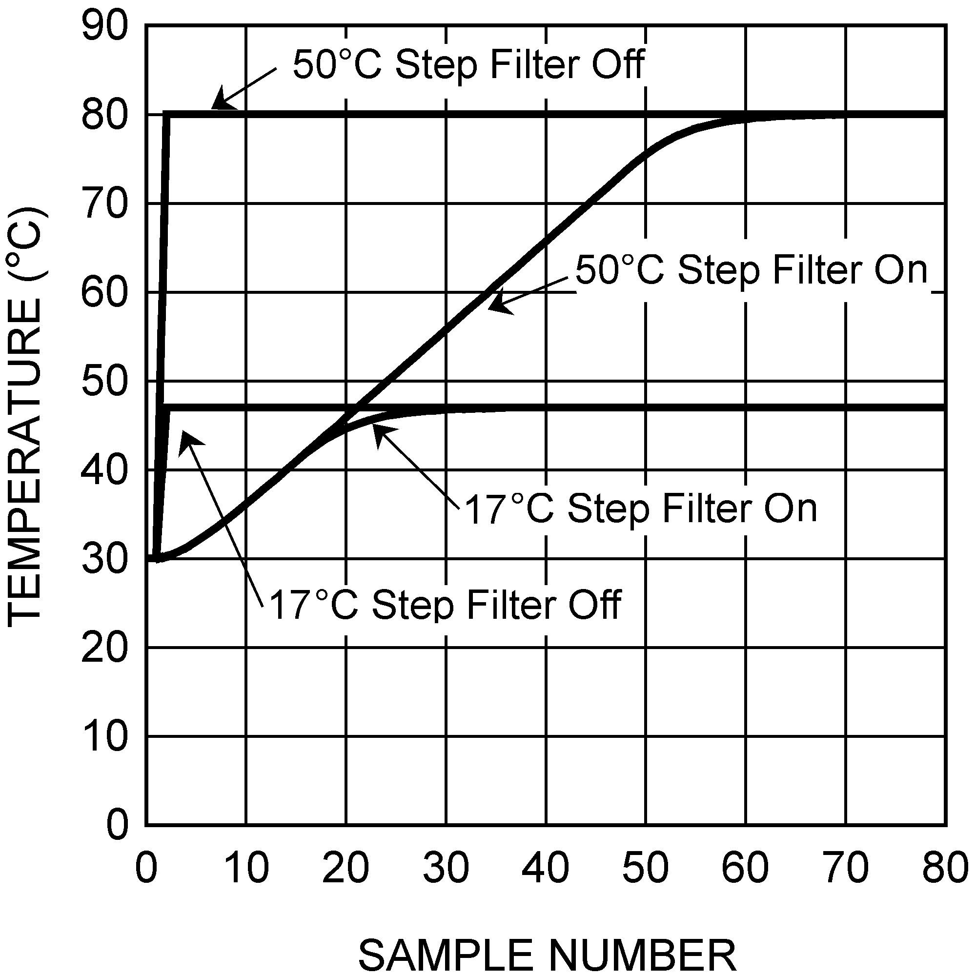 Figure 11. Seventeen and Fifty Degree Step Response
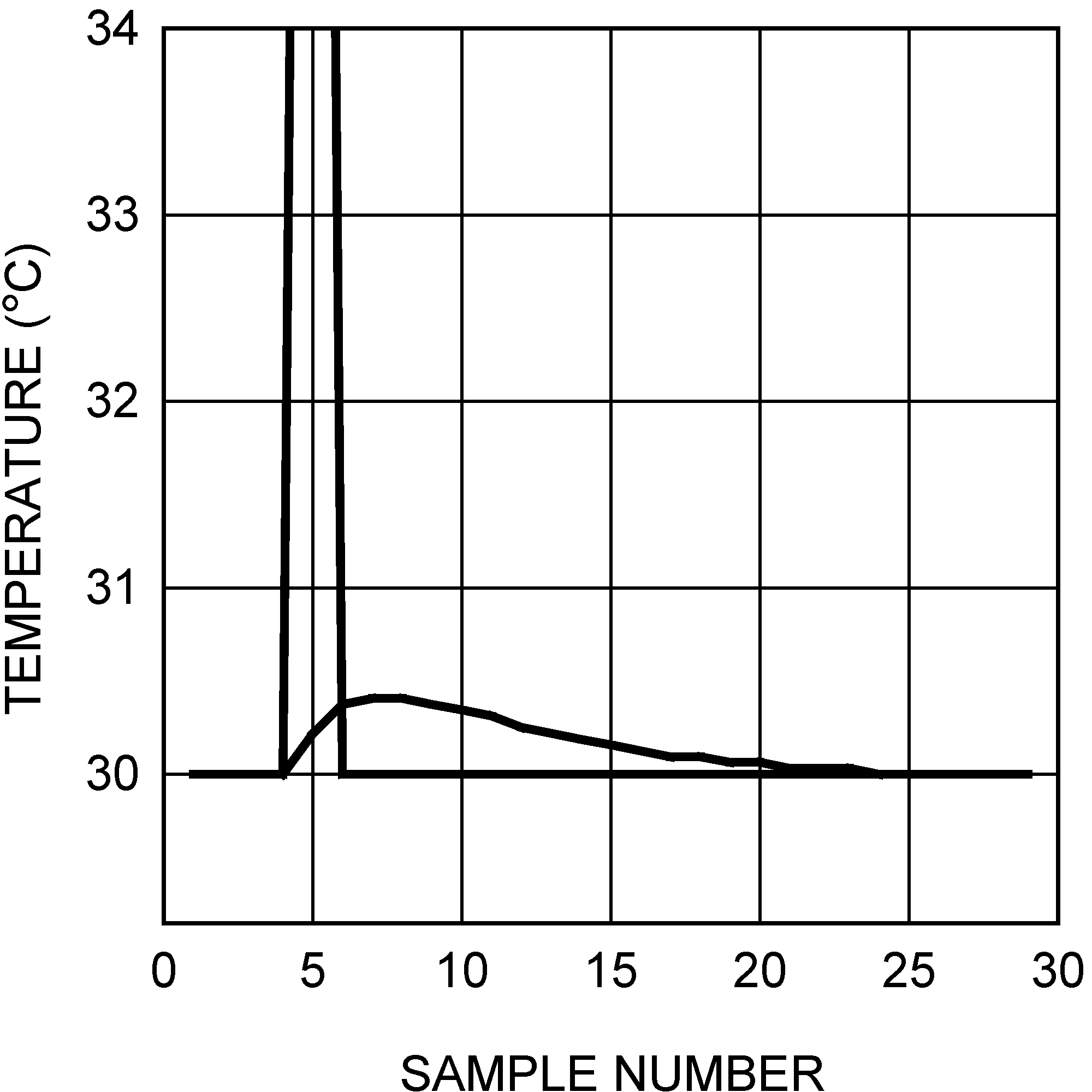 Figure 13. Impulse Response With Input Transients Greater Than 4°C
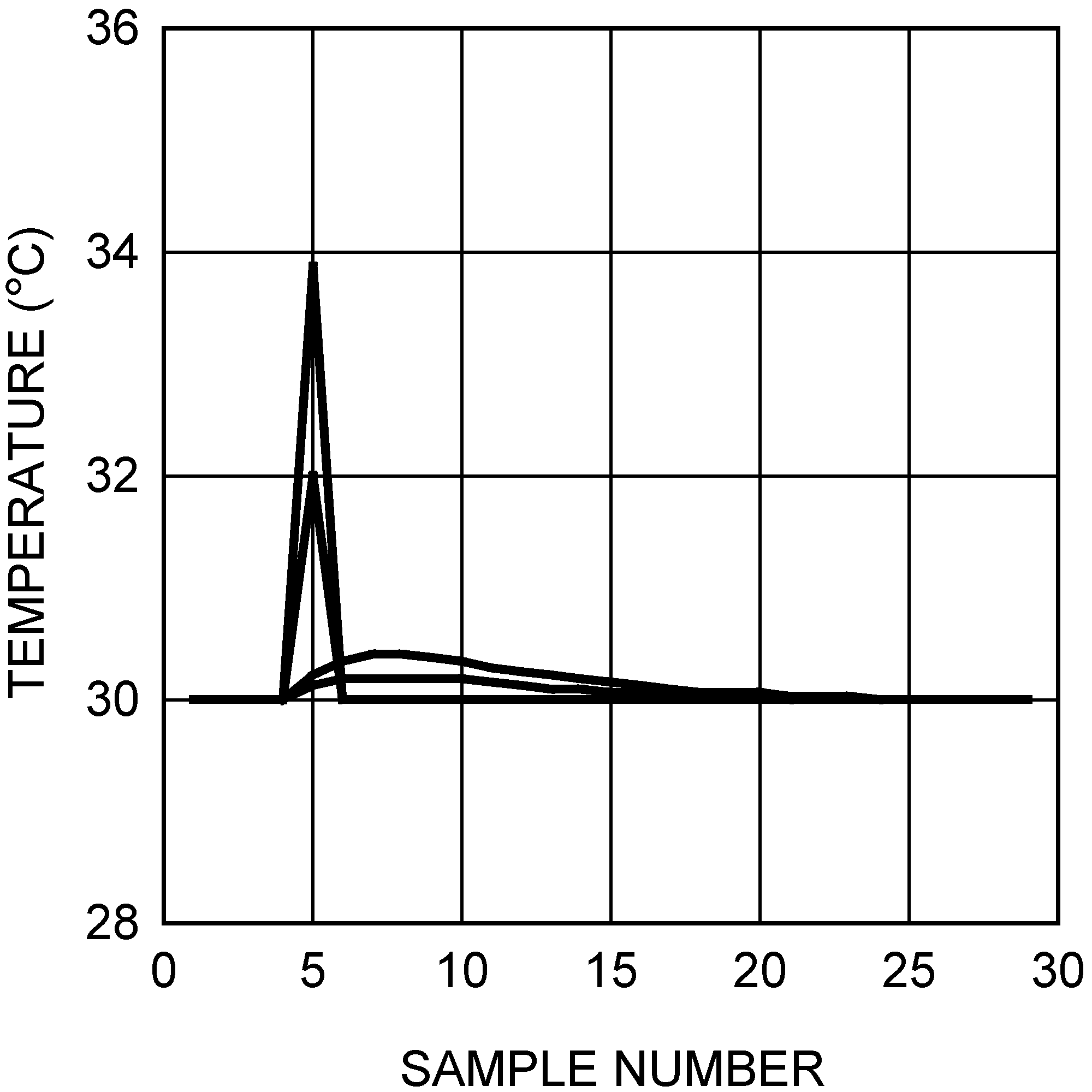 Figure 12. Impulse Response With Input Transients Less Than 4°C
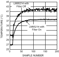 Figure 14. Digital Filter Response in a Typical Intel Processor on a 65 nm or 90 nm Process. The Filter Curves Were Purposely Offset for Clarity.
Figure 14 shows the filter in use in a typical system. Note that the two curves have been purposely offset for clarity. Inserting the filter does not induce an offset as shown.
7.3.5 Fault Queue
To suppress erroneous TCRIT1,TCRIT2 and TCRIT3 triggering the LM95214 incorporates a Fault Queue for the unfiltered remote channels 3 and 4. The Fault Queue acts to ensure the remote temperature measurement of these channels is genuinely beyond the corresponding Tcrit limit by not triggering until three consecutive out of limit measurements have been made, see Figure 15 for an example. The Fault Queue defaults on upon power-up. The fault queue for channels 3 and 4 can be turned ON or OFF through bits 0 and 1 of the Configuration Register. When the fault queue is enabled, the TCRIT1, TCRIT2 and TCRIT3 pins will be triggered if the temperature is above the Tcrit limit for 3 consecutive conversions and the corresponding mask bit is 0 in the TCRIT Mask registers. Similarly the temperature needs to be below the Tcrit limit minus the hysteresis value for three consecutive conversions for the TCRIT1, TCRIT2 and TCRIT3 pins to deactivate.
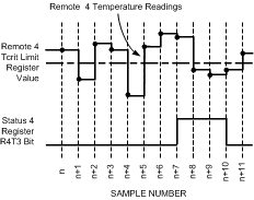 Figure 15. Fault Queue Response Diagram (With 0°C Hysteresis)
7.3.6 Temperature Data Format
Temperature data can only be read from the Local and Remote Temperature value registers. The data format for all temperature values is left justified 16-bit word available in two 8-bit registers. Unused bits will always report 0. All temperature data is clamped and will not roll over when a temperature exceeds full-scale value.
Remote temperature data for all channels can be represented by an 11-bit, two's complement word or unsigned binary word with an LSb (Least Significant Bit) equal to 0.125°C.
Table 5. 11-Bit, 2's Complement (10-Bit Plus Sign)
| TEMPERATURE | DIGITAL OUTPUT | |
|---|---|---|
| BINARY | HEX | |
| +125°C | 0111 1101 0000 0000 | 7D00h |
| +25°C | 0001 1001 0000 0000 | 1900h |
| +1°C | 0000 0001 0000 0000 | 0100h |
| +0.125°C | 0000 0000 0010 0000 | 0020h |
| 0°C | 0000 0000 0000 0000 | 0000h |
| −0.125°C | 1111 1111 1110 0000 | FFE0h |
| −1°C | 1111 1111 0000 0000 | FF00h |
| −25°C | 1110 0111 0000 0000 | E700h |
| −55°C | 1100 1001 0000 0000 | C900h |
Table 6. 11-Bit Unsigned Binary
| TEMPERATURE | DIGITAL OUTPUT | |
|---|---|---|
| BINARY | HEX | |
| +255.875°C | 1111 1111 1110 0000 | FFE0h |
| +255°C | 1111 1111 0000 0000 | FF00h |
| +201°C | 1100 1001 0000 0000 | C900h |
| +125°C | 0111 1101 0000 0000 | 7D00h |
| +25°C | 0001 1001 0000 0000 | 1900h |
| +1°C | 0000 0001 0000 0000 | 0100h |
| +0.125°C | 0000 0000 0010 0000 | 0020h |
| 0°C | 0000 0000 0000 0000 | 0000h |
When the digital filter is enabled on Remote 1 and 2 channels temperature data is represented by a 13-bit unsigned binary or 12-bit plus sign (two's complement) word with an LSb equal to 0.03125°C.
Table 7. 13-Bit, 2's Complement (12-Bit Plus Sign)
| TEMPERATURE | DIGITAL OUTPUT | |
|---|---|---|
| BINARY | HEX | |
| +125°C | 0111 1101 0000 0000 | 7D00h |
| +25°C | 0001 1001 0000 0000 | 1900h |
| +1°C | 0000 0001 0000 0000 | 0100h |
| +0.03125°C | 0000 0000 0000 1000 | 0008h |
| 0°C | 0000 0000 0000 0000 | 0000h |
| −0.03125°C | 1111 1111 1111 1000 | FFF8h |
| −1°C | 1111 1111 0000 0000 | FF00h |
| −25°C | 1110 0111 0000 0000 | E700h |
| −55°C | 1100 1001 0000 0000 | C900h |
Table 8. 13-Bit, Unsigned Binary
| TEMPERATURE | DIGITAL OUTPUT | |
|---|---|---|
| BINARY | HEX | |
| +255.875°C | 1111 1111 1110 0000 | FFE0h |
| +255°C | 1111 1111 0000 0000 | FF00h |
| +201°C | 1100 1001 0000 0000 | C900h |
| +125°C | 0111 1101 0000 0000 | 7D00h |
| +25°C | 0001 1001 0000 0000 | 1900h |
| +1°C | 0000 0001 0000 0000 | 0100h |
| +0.03125°C | 0000 0000 0000 1000 | 0008h |
| 0°C | 0000 0000 0000 0000 | 0000h |
Local Temperature data is only represented by an 11-bit, two's complement, word with an LSb equal to 0.125°C.
Table 9. 11-Bit, 2's Complement (10-Bit Plus Sign)
| TEMPERATURE | DIGITAL OUTPUT | |
|---|---|---|
| BINARY | HEX | |
| +125°C | 0111 1101 0000 0000 | 7D00h |
| +25°C | 0001 1001 0000 0000 | 1900h |
| +1°C | 0000 0001 0000 0000 | 0100h |
| +0.125°C | 0000 0000 0010 0000 | 0020h |
| 0°C | 0000 0000 0000 0000 | 0000h |
| −0.125°C | 1111 1111 1110 0000 | FFE0h |
| −1°C | 1111 1111 0000 0000 | FF00h |
| −25°C | 1110 0111 0000 0000 | E700h |
| −55°C | 1100 1001 0000 0000 | C900h |
7.3.7 SMBDAT Open-Drain Output
The SMBDAT output is an open-drain output and does not have internal pullups. A high level will not be observed on this pin until pullup current is provided by some external source, typically a pullup resistor. Choice of resistor value depends on many system factors but, in general, the pullup resistor must be as large as possible without effecting the SMBus desired data rate. This will minimize any internal temperature reading errors due to internal heating of the LM95214. The maximum resistance of the pullup to provide a 2.1-V high level, based on LM95214 specification for High Level Output Current with the supply voltage at 3 V, is 82 kΩ (5%) or 88.7 kΩ (1%).
7.3.8 TCRIT1, TCRIT2, and TCRIT3 Outputs
The LM95214's TCRIT pins are active-low open-drain outputs and do not include internal pullup resistors. A high level will not be observed on these pins until pullup current is provided by some external source, typically a pullup resistor. Choice of resistor value depends on many system factors but, in general, the pullup resistor must be as large as possible without effecting the performance of the device receiving the signal. This will minimize any internal temperature reading errors due to internal heating of the LM95214. The maximum resistance of the pullup to provide a 2.1-V high level, based on LM95214 specification for High Level Output Current with the supply voltage at 3 V, is 82 kΩ (5%) or 88.7 kΩ (1%). The three TCRIT pins can each sink 6 mA of current and still ensured a Logic Low output voltage of 0.4 V. If all three pins are set at maximum current this will cause a power dissipation of 7.2 mW. This power dissipation combined with a thermal resistance of 77.8°C/W will cause the LM95214's junction temperature to rise approximately 0.6°C and thus cause the Local temperature reading to shift. This can only be cancelled out if the environment that the LM95214 is enclosed in has stable and controlled air flow over the LM95214, as airflow can cause the thermal resistance to change dramatically.
7.3.9 TCRIT Limits and TCRIT Outputs
Figure 16 describes a simplified diagram of the temperature comparison and status register logic. Figure 17, Figure 18, and Figure 19 describe simplified logic diagrams of the circuitry associated with the status registers, mask registers, and the TCRIT output pins.
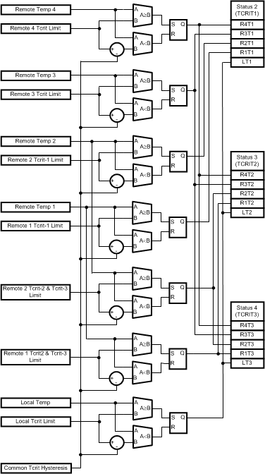 Figure 16. Temperature Comparison Logic and Status Register Simplified Diagram
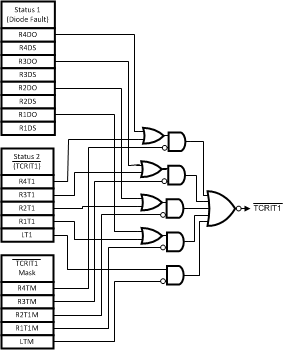 Figure 17. TCRIT1 Mask Register, Status Register 1 and 2, and TCRIT1 Output Logic Diagram
 Figure 19. TCRIT3 Mask Register, Status Register 1 and 4, and TCRIT3 Output Logic Diagram
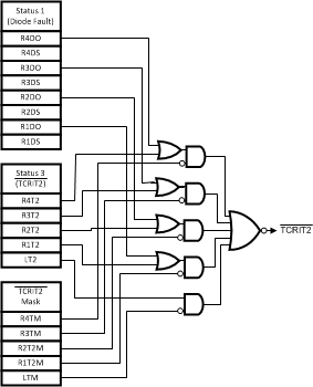 Figure 18. TCRIT2 Mask Register, Status Register 1 and 3, and TCRIT2 Output Logic Diagram
If enabled, local temperature is compared to the user programmable Local Tcrit Limit Register (Default Value = 85°C). The result of this comparison is stored in Status Register 2, Status Register 3 and Status Register 4 (see Figure 16). The comparison result can trigger TCRIT1 pin, TCRIT2 pin or TCRIT3 pin depending on the settings in the TCRIT1 Mask, TCRIT2 Mask and TCRIT3 Mask Registers (see Figure 17, Figure 18, and Figure 19). The comparison result can also be read back from the Status Register 2, Status Register 3 and Status Register 4.
If enabled, remote temperature 1 is compared to the user programmable Remote 1 Tcrit-1 Limit Register (Default Value 110°C) and Remote 1 Tcrit-2 Limit Register (Default Value = 85°C). The result of this comparison is stored in Status Register 2, Status Register 3 and Status Register 4 (see Figure 16). The comparison result can trigger TCRIT1 pin, TCRIT2 pin or TCRIT3 pin depending on the settings in the TCRIT1 Mask, TCRIT2 Mask and TCRIT3 Mask Registers (see Figure 17, Figure 18, and Figure 19). The comparison result can also be read back from the Status Register 2, Status Register 3 and Status Register 4. The remote temperature 2 operates in a similar manner to remote temperature 1 using its associated user programmable limit registers: Remote 2 Tcrit-1 Limit Register (Default Value 110°C) and Remote 2 Tcrit-2 Limit Register (Default Value = 85°C). When enabled, the remote temperature 3 is compared to the user programmable Remote 3 Tcrit Limit Register (Default Value 85°C). The comparison result can trigger TCRIT1 pin, TCRIT2 pin or TCRIT3 pin depending on the settings in the TCRIT1 Mask, TCRIT2 Mask and TCRIT3 Mask Registers. The comparison result can also be read back from the Status Register 2, Status Register 3 and Status Register 4. The remote temperature 4 operates in a similar manner to remote temperature 3 using its associated user programmable limit register: Remote 4 Tcrit Limit Register (Default Value 85°C).
Table 10. Limit Assignments for Each TCRIT Output Pin:
| TCRIT1 | TCRIT2 | TCRIT3 | |
|---|---|---|---|
| Remote 4 | Remote 4 Tcrit Limit |
Remote 4 Tcrit Limit |
Remote 4 Tcrit Limit |
| Remote 3 | Remote 3 Tcrit Limit |
Remote 3 Tcrit Limit |
Remote 3 Tcrit Limit |
| Remote 2 | Remote 2 Tcrit-1 Limit |
Remote 2 Tcrit-2 Limit |
Remote 2 Tcrit-2 Limit |
| Remote 1 | Remote 1 Tcrit-1 Limit |
Remote 1 Tcrit-2 Limit |
Remote 1 Tcrit-2 Limit |
| Local | Local Tcrit Limit |
Local Tcrit Limit |
Local Tcrit Limit |
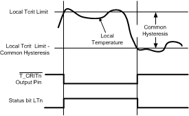 Figure 20. TCRIT Response Diagram (Masking Options Not Included)
The TCRIT response diagram of Figure 20 shows the local temperature interaction with the Tcrit limit and hysteresis value. As can be seen in the diagram when the local temperature exceeds the Tcrit limit register value the LTn Status bit is set and the T_CRITn output(s) is/are activated. The Status bit(s) and outputs are not deactivated until the temperature goes below the value calculated by subtracting the Common Hysteresis value programmed from the limit. This diagram mainly shows an example function of the hysteresis and is not meant to show complete function of the possible settings and options of all the TCRIT outputs and limit values.
7.4 Device Functional Modes
7.4.1 Diode Fault Detection
The LM95214 is equipped with operational circuitry designed to detect fault conditions concerning the remote diodes. In the event that the D+ pin is detected as shorted to GND, D−, VDD or D+ is floating, the Remote Temperature reading is –128.000°C if signed format is selected and 0°C if unsigned format is selected. In addition, the appropriate status register bits RD1M or RD2M (D1 or D0) are set.
7.4.2 Communicating With the LM95214
The data registers in the LM95214 are selected by the Command Register. At power-up the Command Register is set to 00, the location for the Read Local Temperature Register. The Command Register latches the last location it was set to. Each data register in the LM95214 falls into one of three types of user accessibility:
- Read only
- Write only
- Write/Read same address
A Write to the LM95214 will always include the address byte and the command byte. A write to any register requires one data byte.
Reading the LM95214 can take place either of two ways:
- If the location latched in the Command Register is correct (most of the time it is expected that the Command Register will point to one of the Read Temperature Registers because that will be the data most frequently read from the LM95214), then the read can simply consist of an address byte, followed by retrieving the data byte.
- If the Command Register needs to be set, then an address byte, command byte, repeat start, and another address byte will accomplish a read.
The data byte has the most significant bit first. At the end of a read, the LM95214 can accept either acknowledge or No Acknowledge from the Master (No Acknowledge is typically used as a signal for the slave that the Master has read its last byte). It takes the LM95214 190 ms (typical, all channels enabled) to measure the temperature of the remote diodes and internal diode. When retrieving all 11 bits from a previous remote diode temperature measurement, the master must insure that all 11 bits are from the same temperature conversion. This may be achieved by reading the MSB register first. The LSB will be locked after the MSB is read. The LSB will be unlocked after being read. If the user reads MSBs consecutively, each time the MSB is read, the LSB associated with that temperature will be locked in and override the previous LSB value locked-in.
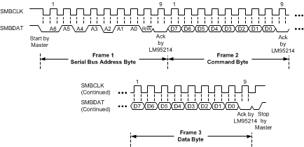 Figure 21. Serial Bus Write to the Internal Command Register Followed by a the Data Byte
 Figure 22. Serial Bus Write to the Internal Command Register
 Figure 23. Serial Bus Read From a Register With the Internal Command Register Preset to Desired Value
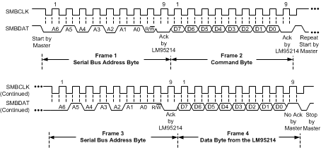 Figure 24. Serial Bus Write Followed by a Repeat Start and Immediate Read
7.4.3 Serial Interface Reset
In the event that the SMBus Master is RESET while the LM95214 is transmitting on the SMBDAT line, the LM95214 must be returned to a known state in the communication protocol. This may be done in one of two ways:
- When SMBDAT is LOW, the LM95214 SMBus state machine resets to the SMBus idle state if either SMBDAT or SMBCLK are held low for more than 35ms (tTIMEOUT). Note that according to SMBus specification 2.0 all devices are to timeout when either the SMBCLK or SMBDAT lines are held low for 25 to 35 ms. Therefore, to insure a timeout of all devices on the bus the SMBCLK or SMBDAT lines must be held low for at least 35 ms.
- When SMBDAT is HIGH, have the master initiate an SMBus start. The LM95214 will respond properly to an SMBus start condition at any point during the communication. After the start the LM95214 will expect an SMBus Address byte.
7.4.4 One-Shot Conversion
The One-Shot register is used to initiate a round of conversions and comparisons when the device is in standby mode, after which the device returns to standby. This is not a data register and it is the write operation that causes the one-shot conversion. The data written to this address is irrelevant and is not stored. A zero will always be read from this register. All the channels that are enabled in the Channel Enable Register will be converted once and the TCRIT1, TCRIT2, and TCRIT3 pins will reflect the comparison results based on this round of conversion results of the channels that are not masked.
7.5 Register Maps
7.5.1 LM95214 Registers
Command register selects which registers will be read from or written to. Data for this register must be transmitted during the Command Byte of the SMBus write communication.
| P7 | P6 | P5 | P4 | P3 | P2 | P1 | P0 |
|---|---|---|---|---|---|---|---|
| Command Byte | |||||||
P0-P7: Command
Table 11. Register Summary
| Register Name | Command Byte (Hex) |
Read/ Write |
D7 | D6 | D5 | D4 | D3 | D2 | D1 | D0 | POR Default (Hex) |
|---|---|---|---|---|---|---|---|---|---|---|---|
| Local Temp MSB | 0x10 | RO | SIGN | 64 | 32 | 16 | 8 | 4 | 2 | 1 | – |
| Local Temp LSB | 0x20 | RO | 1/2 | 1/4 | 1/8 | 0 | 0 | 0 | 0 | 0 | – |
| Remote Temp 1 MSB – Signed | 0x11 | RO | SIGN | 64 | 32 | 16 | 8 | 4 | 2 | 1 | – |
| Remote Temp 1 LSB – Signed, Digital Filter Off | 0x21 | RO | 1/2 | 1/4 | 1/8 | 0 | 0 | 0 | 0 | 0 | – |
| Remote Temp 1 LSB – Signed, Digital Filter On | 1/16 | 1/32 | |||||||||
| Remote Temp 2 MSB – Signed | 0x12 | RO | SIGN | 64 | 32 | 16 | 8 | 4 | 2 | 1 | – |
| Remote Temp 2 LSB – Signed, Digital Filter Off | 0x22 | RO | 1/2 | 1/4 | 1/8 | 0 | 0 | 0 | 0 | 0 | – |
| Remote Temp 2 LSB – Signed, Digital Filter On | 1/16 | 1/32 | |||||||||
| Remote Temp 3 MSB – Signed | 0x13 | RO | SIGN | 64 | 32 | 16 | 8 | 4 | 2 | 1 | – |
| Remote Temp 3 LSB – Signed | 0x23 | RO | 1/2 | 1/4 | 1/8 | 0 | 0 | 0 | 0 | 0 | – |
| Remote Temp 4 MSB – Signed | 0x14 | RO | SIGN | 64 | 32 | 16 | 8 | 4 | 2 | 0 | – |
| Remote Temp 4 LSB – Signed | 0x24 | RO | 1/2 | 1/4 | 1/8 | 0 | 0 | 0 | 0 | 0 | – |
| Remote Temp 1 MSB – Unsigned | 0x19 | RO | 128 | 64 | 32 | 16 | 8 | 4 | 2 | 1 | – |
| Remote Temp 1 LSB – Unsigned, Digital Filter Off | 0x29 | RO | 1/2 | 1/4 | 1/8 | 0 | 0 | 0 | 0 | 0 | – |
| Remote Temp 1 LSB – Unsigned, Digital Filter On | 1/16 | 1/32 | |||||||||
| Remote Temp 2 MSB – Unsigned | 0x1A | RO | 128 | 64 | 32 | 16 | 8 | 4 | 2 | 1 | – |
| Remote Temp 2 LSB – Unsigned, Digital Filter Off | 0x2A | RO | 1/2 | 1/4 | 1/8 | 0 | 0 | 0 | 0 | 0 | – |
| Remote Temp 2 LSB – Unsigned, Digital Filter On | 1/16 | 1/32 | |||||||||
| Remote Temp 3 MSB – Unsigned | 0x1B | RO | 128 | 64 | 32 | 16 | 8 | 4 | 2 | 1 | – |
| Remote Temp 3 LSB – Unsigned | 0x2B | RO | 1/2 | 1/4 | 1/8 | 0 | 0 | 0 | 0 | 0 | – |
| Remote Temp 4 MSB – Unsigned | 0x1C | RO | 128 | 64 | 32 | 16 | 8 | 4 | 2 | 1 | – |
| Remote Temp 4 LSB – Unsigned | 0x2C | RO | 1/2 | 1/4 | 1/8 | 0 | 0 | 0 | 0 | 0 | – |
| Remote 1 Offset | 0x31 | R/W | SIGN | 32 | 16 | 8 | 4 | 2 | 1 | 1/2 | 0x00 |
| Remote 2 Offset | 0x32 | R/W | SIGN | 32 | 16 | 8 | 4 | 2 | 1 | 1/2 | 0x00 |
| Remote 3 Offset | 0x33 | R/W | SIGN | 32 | 16 | 8 | 4 | 2 | 1 | 1/2 | 0x00 |
| Remote 4 Offset | 0x34 | R/W | SIGN | 32 | 16 | 8 | 4 | 2 | 1 | 1/2 | 0x00 |
| Configuration | 0x03 | R/W | – | STBY | – | – | – | – | R4QE | R3QE | 0x03 |
| Conversion Rate | 0x04 | R/W | – | – | – | – | – | – | CR1 | CR0 | 0x02 |
| Channel Conversion Enable | 0x05 | R/W | – | – | – | R4CE | R3CE | R2CE | R1CE | LCE | 0x1F |
| Filter Setting | 0x06 | R/W | – | – | – | – | R2F1 | R2F0 | R1F1 | R1F0 | 0x0F |
| 1-shot | 0x0F | WO | – | – | – | – | – | – | – | – | – |
| Common Status Register | 0x02 | RO | BUSY | NR | – | – | SR4F | SR3F | SR2F | SR1F | 0x00 |
| Status 1 (Diode Fault) | 0x07 | RO | R4DO | R4DS | R3DO | R3DS | R2DO | R2DS | R1DO | R1DS | – |
| Status 2 (TCRIT1) | 0x08 | RO | – | – | – | R4T1 | R3T1 | R2T1 | R1T1 | LT1 | – |
| Status 3 (TCRIT2) | 0x09 | RO | – | – | – | R4T2 | R3T2 | R2T2 | R1T2 | LT2 | – |
| Status 4 (TCRIT3) | 0x0A | RO | – | – | – | R4T3 | R3T3 | R2T3 | R1T3 | LT3 | – |
| TCRIT1 Mask | 0x0C | R/W | – | – | – | R4TM | R3TM | R2T1M | R1T1M | LTM | 0x19 |
| TCRIT2 Mask | 0x0D | R/W | – | – | – | R4TM | R3TM | R2T2M | R1T2M | LTM | 0x00 |
| TCRIT3 Mask | 0x0E | R/W | – | – | – | R4TM | R3TM | R2T2M | R1T2M | LTM | 0x07 |
| Local Tcrit Limit | 0x40 | R/W | 0 | 64 | 32 | 16 | 8 | 4 | 2 | 1 | 0x55 |
| Remote 1 Tcrit-1 Limit | 0x41 | R/W | 128 | 64 | 32 | 16 | 8 | 4 | 2 | 1 | 0x6E |
| Remote 2 Tcrit-1 Limit | 0x42 | R/W | 128 | 64 | 32 | 16 | 8 | 4 | 2 | 1 | 0x6E |
| Remote 3 Tcrit Limit | 0x43 | R/W | 128 | 64 | 32 | 16 | 8 | 4 | 2 | 1 | 0x55 |
| Remote 4 Tcrit Limit | 0x44 | R/W | 128 | 64 | 32 | 16 | 8 | 4 | 2 | 1 | 0x55 |
| Remote 1 Tcrit-2 and Tcrit-3 Limit | 0x49 | R/W | 128 | 64 | 32 | 16 | 8 | 4 | 2 | 1 | 0x55 |
| Remote 2 Tcrit-2 and Tcrit-3 Limit | 0x4A | R/W | 128 | 64 | 32 | 16 | 8 | 4 | 2 | 1 | 0x55 |
| Common Tcrit Hysteresis | 0x5A | R/W | 0 | 0 | 0 | 16 | 8 | 4 | 2 | 1 | 0x0A |
| Manufacturer ID | 0xFE | RO | 0 | 0 | 0 | 0 | 0 | 0 | 0 | 1 | 0x01 |
| Revision ID | 0xFF | RO | 0 | 1 | 1 | 1 | 1 | 0 | 0 | 1 | 0x79 |
7.5.1.1 Value Registers
For data synchronization purposes, the MSB register must be read first if the user wants to read both MSB and LSB registers. The LSB will be locked after the MSB is read. The LSB will be unlocked after being read. If the user reads MSBs consecutively, each time the MSB is read, the LSB associated with that temperature will be locked in and override the previous LSB value locked-in
7.5.1.1.1 Local Value Registers
| Register Name | Command Byte (Hex) |
Read/ Write |
D7 | D6 | D5 | D4 | D3 | D2 | D1 | D0 | POR Default (Hex) |
|---|---|---|---|---|---|---|---|---|---|---|---|
| Local Temp MSB | 0x10 | RO | SIGN | 64 | 32 | 16 | 8 | 4 | 2 | 1 | – |
| Local Temp LSB | 0x20 | RO | 1/2 | 1/4 | 1/8 | 0 | 0 | 0 | 0 | 0 | – |
| Bit(s) | Bit Name | Read/Write | Description | |
|---|---|---|---|---|
| 7 | SIGN | RO | Sign bit | The Local temperature MSB value register range is +127°C to −128°C. The value programmed in this register is used to determine a local temperature error event. |
| 6 | 64 | RO | bit weight 64°C | |
| 5 | 32 | RO | bit weight 32°C | |
| 4 | 16 | RO | bit weight 16°C | |
| 3 | 8 | RO | bit weight 8°C | |
| 2 | 4 | RO | bit weight 4°C | |
| 1 | 2 | RO | bit weight 2°C | |
| 0 | 1 | RO | bit weight 1°C | |
| Bit(s) | Bit Name | Read/Write | Description | |
|---|---|---|---|---|
| 7 | 1/2 | RO | bit weight 1/2°C (0.5°C) | The Local Limit register range is 0°C to 127°C. The value programmed in this register is used to determine a local temperature error event. |
| 6 | 1/4 | RO | bit weight 1/4°C (0.25°C) | |
| 5 | 1/8 | RO | bit weight 1/8°C (0.125°C) | |
| 4-0 | 0 | RO | Reserved – will report 0 when read. | |
7.5.1.1.2 Remote Temperature Value Registers With Signed Format
| Register Name | Command Byte (Hex) |
Read/ Write |
D7 | D6 | D5 | D4 | D3 | D2 | D1 | D0 | POR Default (Hex) |
|---|---|---|---|---|---|---|---|---|---|---|---|
| Remote Temp 1 MSB – Signed | 0x11 | RO | SIGN | 64 | 32 | 16 | 8 | 4 | 2 | 1 | – |
| Remote Temp 1 LSB – Signed, Digital Filter Off | 0x21 | RO | 1/2 | 1/8 | 0 | 0 | 0 | 0 | 0 | 0 | – |
| Remote Temp 1 LSB – Signed, Digital Filter On | 1/16 | 1/32 | |||||||||
| Remote Temp 2 MSB – Signed | 0x12 | RO | SIGN | 64 | 32 | 16 | 8 | 4 | 2 | 1 | – |
| Remote Temp 2 LSB – Signed, Digital Filter Off | 0x22 | RO | 1/2 | 1/8 | 0 | 0 | 0 | 0 | 0 | 0 | – |
| Remote Temp 2 LSB – Signed, Digital Filter On | 1/16 | 1/32 | |||||||||
| Remote Temp 3 MSB – Signed | 0x13 | RO | SIGN | 64 | 32 | 16 | 8 | 4 | 2 | 1 | – |
| Remote Temp 3 LSB – Signed | 0x23 | RO | 1/2 | 1/8 | 0 | 0 | 0 | 0 | 0 | 0 | – |
| Remote Temp 4 MSB – Signed | 0x14 | RO | SIGN | 64 | 32 | 16 | 8 | 4 | 2 | 0 | – |
| Remote Temp 4 LSB – Signed | 0x24 | RO | 1/2 | 1/8 | 0 | 0 | 0 | 0 | 0 | 0 | – |
The Local temperature MSB value register range is +127°C to −128°C. The value programmed in this register is used to determine a local temperature error event.
| Bit(s) | Bit Name | Read/Write | Description |
|---|---|---|---|
| 7 | SIGN | RO | Sign bit |
| 6 | 64 | RO | bit weight 64°C |
| 5 | 32 | RO | bit weight 32°C |
| 4 | 16 | RO | bit weight 16°C |
| 3 | 8 | RO | bit weight 8°C |
| 2 | 4 | RO | bit weight 4°C |
| 1 | 2 | RO | bit weight 2°C |
| 0 | 1 | RO | bit weight 1°C |
| Bit(s) | Bit Name | Read/Write | Description |
|---|---|---|---|
| 7 | 1/2 | RO | bit weight 1/2°C (0.5°C) |
| 6 | 1/4 | RO | bit weight 1/4°C (0.25°C) |
| 5 | 1/8 | RO | bit weight 1/8°C (0.125°C) |
| 4 | 0 or 1/16 | RO | When the digital filter is disabled this bit will always read 0. When the digital filter is enabled this bit will report 1/16°C (0.0625°C) bit state. |
| 3 | 0 or 1/32 | RO | When the digital filter is disabled this bit will always read 0. When the digital filter is enabled this bit will report 1/32°C (0.03125°C) bit state. |
| 2-0 | 0 | RO | Reserved – will report 0 when read. |
7.5.1.1.3 Remote Temperature Value Registers With Unsigned Format
| Register Name | Command Byte (Hex) |
Read/ Write |
D7 | D6 | D5 | D4 | D3 | D2 | D1 | D0 | POR Default (Hex) |
|---|---|---|---|---|---|---|---|---|---|---|---|
| Remote Temp 1 MSB – Unsigned | 0x19 | RO | 128 | 64 | 32 | 16 | 8 | 4 | 2 | 1 | – |
| Remote Temp 1 LSB – Unsigned, Digital Filter Off | 0x29 | RO | 1/2 | 1/8 | 0 | 0 | 0 | 0 | 0 | 0 | – |
| Remote Temp 1 LSB – Unsigned, Digital Filter On | 1/16 | 1/32 | |||||||||
| Remote Temp 2 MSB – Unsigned | 0x1A | RO | 128 | 64 | 32 | 16 | 8 | 4 | 2 | 1 | – |
| Remote Temp 2 LSB – Unsigned, Digital Filter Off | 0x2A | RO | 1/2 | 1/8 | 0 | 0 | 0 | 0 | 0 | 0 | – |
| Remote Temp 2 LSB – Unsigned, Digital Filter On | 1/16 | 1/32 | |||||||||
| Remote Temp 3 MSB – Unsigned | 0x1B | RO | 128 | 64 | 32 | 16 | 8 | 4 | 2 | 1 | – |
| Remote Temp 3 LSB – Unsigned | 0x2B | RO | 1/2 | 1/8 | 0 | 0 | 0 | 0 | 0 | 0 | – |
| Remote Temp 4 MSB – Unsigned | 0x1C | RO | 128 | 64 | 32 | 16 | 8 | 4 | 2 | 1 | – |
| Remote Temp 4 LSB – Unsigned | 0x2C | RO | 1/2 | 1/8 | 0 | 0 | 0 | 0 | 0 | 0 | – |
| Bit(s) | Bit Name | Read/Write | Description |
|---|---|---|---|
| 7 | SIGN | RO | bit weight 128°C |
| 6 | 64 | RO | bit weight 64°C |
| 5 | 32 | RO | bit weight 32°C |
| 4 | 16 | RO | bit weight 16°C |
| 3 | 8 | RO | bit weight 8°C |
| 2 | 4 | RO | bit weight 4°C |
| 1 | 2 | RO | bit weight 2°C |
| 0 | 1 | RO | bit weight 1°C |
| Bit(s) | Bit Name | Read/Write | Description |
|---|---|---|---|
| 7 | 1/2 | RO | bit weight 1/2°C (0.5°C) |
| 6 | 1/4 | RO | bit weight 1/4°C (0.25°C) |
| 5 | 1/8 | RO | bit weight 1/8°C (0.125°C) |
| 4 | 0 or 1/16 | RO | When the digital filter is disabled this bit will always read 0. When the digital filter is enabled this bit will report 1/16°C (0.0625°C) bit state. |
| 3 | 0 or 1/32 | RO | When the digital filter is disabled this bit will always read 0. When the digital filter is enabled this bit will report 1/32°C (0.03125°C) bit state. |
| 2-0 | 0 | RO | Reserved – will report 0 when read. |
7.5.1.2 Diode Configuration Register
7.5.1.2.1 Remote 1-4 Offset
| Register Name | Command Byte (Hex) |
Read/ Write |
D7 | D6 | D5 | D4 | D3 | D2 | D1 | D0 | POR Default (Hex) |
|---|---|---|---|---|---|---|---|---|---|---|---|
| Remote 1 Offset | 0x31 | R/W | SIGN | 32 | 16 | 8 | 4 | 2 | 1 | 1/2 | 0x00 |
| Remote 2 Offset | 0x32 | R/W | SIGN | 32 | 16 | 8 | 4 | 2 | 1 | 1/2 | 0x00 |
| Remote 3 Offset | 0x33 | R/W | SIGN | 32 | 16 | 8 | 4 | 2 | 1 | 1/2 | 0x00 |
| Remote 4 Offset | 0x34 | R/W | SIGN | 32 | 16 | 8 | 4 | 2 | 1 | 1/2 | 0x00 |
| Bit(s) | Bit Name | Read/Write | Description | |
|---|---|---|---|---|
| 7 | SIGN | R/W | Sign bit | All registers have 2’s complement format. The offset range for each remote is +63.5°C/−64°C. The value programmed in this register is directly added to the actual reading of the ADC and the modified number is reported in the remote value registers. |
| 6 | 32 | R/W | bit weight 32°C | |
| 5 | 16 | R/W | bit weight 16°C | |
| 4 | 8 | R/W | bit weight 8°C | |
| 3 | 4 | R/W | bit weight 4°C | |
| 2 | 2 | R/W | bit weight 2°C | |
| 1 | 1 | R/W | bit weight 1°C | |
| 0 | 1/2 | R/W | bit weight 1/2°C (0.5°C) | |
7.5.1.3 Configuration Registers
7.5.1.3.1 Main Configuration Register
| Register Name | Command Byte (Hex) |
Read/ Write |
D7 | D6 | D5 | D4 | D3 | D2 | D1 | D0 | POR Default (Hex) |
|---|---|---|---|---|---|---|---|---|---|---|---|
| Configuration | 0×03 | R/W | – | STBY | – | – | – | – | R4QE | R3QE | 0×03 |
| Bit(s) | Bit Name | Read/Write | Description |
|---|---|---|---|
| 7 | – | RO | Reserved will report 0 when read. |
| 6 | STBY | R/W | Software Standby 1 – standby (when in this mode one conversion sequence can be initiated by writing to the one-shot register) 0 – active/converting |
| 5–2 | – | RO | Reserved – will report 0 when read. |
| 1 | R4QE | R/W | Fault queue enable for Remote 4 1– Fault queue enabled 0– Fault queue disabled |
| 0 | R3QE | R/W | Fault queue enable for Remote 3 1– Fault queue enabled 0– Fault queue disabled |
7.5.1.3.2 Conversion Rate Register
| Register Name | Command Byte (Hex) |
Read/ Write |
D7 | D6 | D5 | D4 | D3 | D2 | D1 | D0 | POR Default (Hex) |
|---|---|---|---|---|---|---|---|---|---|---|---|
| Conversion Rate | 0×04 | R/W | – | – | – | – | – | – | CR1 | CR0 | 0×02 |
| Bit(s) | Bit Name | Read/Write | Description | |
|---|---|---|---|---|
| 7-2 | – | RO | Reserved – will report 0 when read. | |
| 1-0 | CR[1:0] | R/W | Conversion rate control bits modify the time interval for conversion of the channels enabled. The channels enabled are converted sequentially then standby mode enabled for the remainder of the time interval. | |
| CR[1:0] | Conversion Rate | |||
| 00 | continuous (30 ms to 143 ms) | |||
| 01 | 0.364 s | |||
| 10 | 1s | |||
| 11 | 2.5 s | |||
7.5.1.3.3 Channel Conversion Enable
When a conversion is disabled for a particular channel it is skipped. The continuous conversion rate is effected all other conversion rates are not effected as extra standby time is inserted to compensate. See Conversion Rate Register description.
| Register Name | Command Byte (Hex) |
Read/ Write |
D7 | D6 | D5 | D4 | D3 | D2 | D1 | D0 | POR Default (Hex) |
|---|---|---|---|---|---|---|---|---|---|---|---|
| Channel Conversion Enable | 0×05 | R/W | – | – | – | R4CE | R3CE | R2CE | R1CE | LCE | 0×1F |
| Bit(s) | Bit Name | Read/Write | Description |
|---|---|---|---|
| 7–5 | – | RO | Reserved – will report 0 when read. |
| 4 | R4CE | R/W | Remote 4 Temperature Conversion Enable 1– Remote 4 temp conversion enabled 0– Remote 4 temp conversion disabled |
| 3 | R3CE | R/W | Remote 3 Temperature Conversion Enable 1– Remote 3 temp conversion enabled 0– Remote 3 temp conversion disabled |
| 2 | R2CE | R/W | Remote 2 Temperature Conversion Enable 1– Remote 2 temp conversion enabled 0– Remote 2 temp conversion disabled |
| 1 | R1CE | R/W | Remote 1 Temperature Conversion Enable 1– Remote 1 temp conversion enabled 0– Remote 1 temp conversion disabled |
| 0 | LCE | R/W | Local Temperature Conversion Enable 1– Local temp conversion enabled 0– Local temp conversion disabled |
7.5.1.3.4 Filter Setting
| Register Name | Command Byte (Hex) |
Read/ Write |
D7 | D6 | D5 | D4 | D3 | D2 | D1 | D0 | POR Default (Hex) |
|---|---|---|---|---|---|---|---|---|---|---|---|
| Filter Setting | 0x06 | R/W | – | – | – | – | R2F1 | R2F0 | R1F1 | R1F0 | 0x0F |
| Bit(s) | Bit Name | Read/Write | Description | |
|---|---|---|---|---|
| 7–4 | – | RO | Reserved – will report 0 when read. | |
| 3–2 | R2F[1:0] | R/W | Remote Channel 2 Filter Enable Bits | |
| R2F[1:0] | Digital Filter State | |||
| 00 | disable all digital filtering | |||
| 01 | enable basic filter | |||
| 10 | reserved (do not use) | |||
| 11 | enable enhanced filter | |||
| 1–0 | R1F[1:0] | R/W | Remote Channel 1 Filter Enable | |
| R1F[1:0] | Filter State | |||
| 00 | disable all digital filtering | |||
| 01 | enable basic filter | |||
| 10 | reserved (do not use) | |||
| 11 | enable enhanced filter | |||
7.5.1.3.5 1-Shot
| Register Name | Command Byte (Hex) |
Read/ Write |
D7 | D6 | D5 | D4 | D3 | D2 | D1 | D0 | POR Default (Hex) |
|---|---|---|---|---|---|---|---|---|---|---|---|
| 1-Shot | 0×0F | WO | – | – | – | – | – | – | – | – | – |
| Bit(s) | Bit Name | Read/Write | Description |
|---|---|---|---|
| 7–0 | - | WO | Writing to this register activates one conversion for all the enabled channels if the chip is in standby mode (that is,. standby bit = 1). The actual data written does not matter and is not stored. |
7.5.1.4 Status Registers
7.5.1.4.1 Common Status Register
| Register Name | Command Byte (Hex) |
Read/ Write |
D7 | D6 | D5 | D4 | D3 | D2 | D1 | D0 | POR Default (Hex) |
|---|---|---|---|---|---|---|---|---|---|---|---|
| Common Status Register | 0×02 | RO | BUSY | NR | – | – | SR4F | SR3F | SR2F | SR1F | 0×00 |
| Bit(s) | Bit Name | Read/Write | Description |
|---|---|---|---|
| 7 | BUSY | RO | Busy bit (device converting) |
| 6 | NR | RO | Not Ready bit (30 ms), indicates power up initialization sequence is in progress |
| 5–4 | – | RO | Reserved – will report 0 when read. |
| 3 | SR4F | RO | Status Register 4 Flag: 1 – indicates that Status Register 4 has at least one bit set 0 – indicates that all of Status Register 4 bits are cleared |
| 2 | SR3F | RO | Status Register 3 Flag: 1 – indicates that Status Register 3 has at least one bit set 0 – indicates that all of Status Register 3 bits are cleared |
| 1 | SR2F | RO | Status Register 2 Flag: 1 – indicates that Status Register 2 has at least one bit set 0 – indicates that all of Status Register 2 bits are cleared |
| 0 | SR1F | RO | Status Register 1 Flag: 1 – indicates that Status Register 1 has at least one bit set 0 – indicates that all of Status Register 1 bits are cleared |
7.5.1.4.2 Status 1 Register (Diode Fault)
Status fault bits for open or shorted diode (that is,. Short Fault: D+ shorted to Ground or D-; Open Fault: D+ shorted to VDD, or floating). During fault conditions the temperature reading is 0 °C if unsigned value registers are read or –128.000 °C if signed value registers are read.
| Register Name | Command Byte (Hex) |
Read/ Write |
D7 | D6 | D5 | D4 | D3 | D2 | D1 | D0 | POR Default (Hex) |
|---|---|---|---|---|---|---|---|---|---|---|---|
| Status 1 (Diode Fault) | 0×07 | RO | R4DO | R4DS | R3DO | R3DS | R2DO | R2DS | R1DO | R1DS | – |
| Bit(s) | Bit Name | Read/Write | Description |
|---|---|---|---|
| 7 | R4DO | RO | Remote 4 diode open fault status: 1 – indicates that remote 4 diode has an "open" fault 0 – indicates that remote 4 diode does not have an "open" fault |
| 6 | R4DS | RO | Remote 4 diode short fault status: 1 – indicates that remote 4 diode has a "short" fault 0 – indicates that remote 4 diode does not have a "short" fault |
| 5 | R3DO | RO | Remote 3 diode open fault status: 1 – indicates that remote 3 diode has an "open" fault 0 – indicates that remote 3 diode does not have an "open" fault |
| 4 | R3DS | RO | Remote 3 diode short fault status: 1 – indicates that remote 3 diode has a "short" fault 0 – indicates that remote 3 diode does not have a "short" fault |
| 3 | R2DO | RO | Remote 2 diode open fault status: 1 – indicates that remote 2 diode has an "open" fault 0 – indicates that remote 2 diode does not have an "open" fault |
| 2 | R2DS | RO | Remote 2 diode short fault status: 1 – indicates that remote 2 diode has a "short" fault 0 – indicates that remote 2 diode does not have a "short" fault |
| 1 | R1DO | RO | Remote 1 diode open fault status: 1 – indicates that remote 1 diode has an "open" fault 0 – indicates that remote 1 diode does not have an "open" fault |
| 0 | R1DS | RO | Remote 1 diode short fault status: 1 – indicates that remote 1 diode has a "short" fault 0 – indicates that remote 1 diode does not have a "short" fault |
7.5.1.4.3 Status 2 (TCRIT1)
Status bits for TCRIT1. When one or more of these bits are set and if not masked the TCRIT1 output will activate. TCRIT1 will deactivate when all these bits are cleared.
| Register Name | Command Byte (Hex) |
Read/ Write |
D7 | D6 | D5 | D4 | D3 | D2 | D1 | D0 | POR Default (Hex) |
|---|---|---|---|---|---|---|---|---|---|---|---|
| Status 2 (TCRIT1) | 0×08 | RO | – | – | – | R4T1 | R3T1 | R2T1 | R1T1 | LT1 | – |
| Bit(s) | Bit Name | Read/Write | Description |
|---|---|---|---|
| 7–5 | - | RO | Reserved – will report 0 when read. |
| 4 | R4T1 | RO | Remote 4 Tcrit Status: 1 – indicates that remote 4 reading is greater than or equal to the value set in Remote 4 Tcrit Limit register 0 – indicates that that remote 4 reading is less than the value set in Remote 4 Tcrit Limit register minus the Common Hysteresis value |
| 3 | R3T1 | RO | Remote 3 Tcrit Status: 1 – indicates that remote 3 reading is greater than or equal to the value set in Remote 3 Tcrit Limit register 0 – indicates that that remote 3 reading is less than the value set in Remote 3 Tcrit Limit register minus the Common Hysteresis value |
| 2 | R2T1 | RO | Remote 2 Tcrit-1 Status: 1 – indicates that remote 2 reading is greater than or equal to the value set in Remote 2 Tcrit-1 Limit register 0 – indicates that that remote 2 reading is less than the value set in Remote 2 Tcrit-1 Limit register minus the Common Hysteresis value |
| 1 | R1T1 | RO | Remote 1 Tcrit-1 Status: 1 – indicates that remote 1 reading is greater than or equal to the value set in Remote 1 Tcrit-1 Limit register 0 – indicates that that remote 1 reading is less than the value set in Remote 1 Tcrit-1 Limit register minus the Common Hysteresis value |
| 0 | LT1 | RO | Local Tcrit Status: 1 – indicates that local reading is greater than or equal to the value set in Local Tcrit Limit register 0 – indicates that local reading is less than the value set in Local Tcrit Limit register minus the Common Hysteresis value |
7.5.1.4.4 Status 3 (TCRIT2)
Status bits for TCRIT2. When one or more of these bits are set and if not masked the TCRIT2 output will activate. TCRIT2 will deactivate when all these bits are cleared.
| Register Name | Command Byte (Hex) |
Read/ Write |
D7 | D6 | D5 | D4 | D3 | D2 | D1 | D0 | POR Default (Hex) |
|---|---|---|---|---|---|---|---|---|---|---|---|
| Status 3 (TCRIT2) | 0×09 | RO | – | – | – | R4T2 | R3T2 | R2T2 | R1T2 | LT2 | – |
| Bit(s) | Bit Name | Read/Write | Description |
|---|---|---|---|
| 7–5 | - | RO | Reserved – will report 0 when read. |
| 4 | R4T2 | RO | Remote 4 Tcrit Status: 1 – indicates that remote 4 reading is greater than or equal to the value set in Remote 4 Tcrit Limit register 0 – indicates that that remote 4 reading is less than the value set in Remote 4 Tcrit Limit register minus the Common Hysteresis value |
| 3 | R3T2 | RO | Remote 3 Tcrit Status: 1 – indicates that remote 3 reading is greater than or equal to the value set in Remote 3 Tcrit Limit register 0 – indicates that that remote 3 reading is less than the value set in Remote 3 Tcrit Limit register minus the Common Hysteresis value |
| 2 | R2T2 | RO | Remote 2 Tcrit-2 Status: 1 – indicates that remote 2 reading is greater than or equal to the value set in Remote 2 Tcrit-2 Limit register 0 – indicates that that remote 2 reading is less than the value set in Remote 2 Tcrit-2 Limit register minus the Common Hysteresis value |
| 1 | R1T2 | RO | Remote 1 Tcrit-2 Status: 1 – indicates that remote 1 reading is greater than or equal to the value set in Remote 1 Tcrit-2 Limit register 0 – indicates that that remote 1 reading is less than the value set in Remote 1 Tcrit-2 Limit register minus the Common Hysteresis value |
| 0 | LT2 | RO | Local Tcrit Status: 1 – indicates that local reading is greater than or equal to the value set in Local Tcrit Limit register 0 – indicates that local reading is less than the value set in Local Tcrit Limit register minus the Common Hysteresis value |
7.5.1.4.5 Status 4 (TCRIT3)
Status bits for TCRIT3. When one or more of these bits are set and if not masked the TCRIT3 output will activate. TCRIT3 will deactivate when all these bits are cleared.
| Register Name | Command Byte (Hex) |
Read/ Write |
D7 | D6 | D5 | D4 | D3 | D2 | D1 | D0 | POR Default (Hex) |
|---|---|---|---|---|---|---|---|---|---|---|---|
| Status 4 (TCRIT3) | 0×0A | RO | – | – | – | R4T3 | R3T3 | R2T3 | R1T3 | LT3 | – |
| Bit(s) | Bit Name | Read/Write | Description |
|---|---|---|---|
| 7–5 | - | RO | Reserved – will report 0 when read. |
| 4 | R4T3 | RO | Remote 4 Tcrit Status: 1 – indicates that remote 4 reading is greater than or equal to the value set in Remote 4 Tcrit Limit register 0 – indicates that that remote 4 reading is less than the value set in Remote 4 Tcrit Limit register minus the Common Hysteresis value |
| 3 | R3T3 | RO | Remote 3 Tcrit Status: 1 – indicates that remote 3 reading is greater than or equal to the value set in Remote 3 Tcrit Limit register 0 – indicates that that remote 3 reading is less than the value set in Remote 3 Tcrit Limit register minus the Common Hysteresis value |
| 2 | R2T3 | RO | Remote 2 Tcrit-2 Status: 1 – indicates that remote 2 reading is greater than or equal to the value set in Remote 2 Tcrit-2 Limit register 0 – indicates that that remote 2 reading is less than the value set in Remote 2 Tcrit-2 Limit register minus the Common Hysteresis value |
| 1 | R1T3 | RO | Remote 1 Tcrit-2 Status: 1 – indicates that remote 1 reading is greater than or equal to the value set in Remote 1 Tcrit-2 Limit register 0 – indicates that that remote 1 reading is less than the value set in Remote 1 Tcrit-2 Limit register minus the Common Hysteresis value |
| 0 | LT3 | RO | Local Tcrit Status: 1 – indicates that local reading is greater than or equal to the value set in Local Tcrit Limit register 0 – indicates that local reading is less than the value set in Local Tcrit Limit register minus the Common Hysteresis value |
7.5.1.5 Mask Registers
7.5.1.5.1 TCRIT1 Mask Register
The mask bits in this register allow control over which error events propagate to the TCRIT1 pin.
| Register Name | Command Byte (Hex) |
Read/ Write |
D7 | D6 | D5 | D4 | D3 | D2 | D1 | D0 | POR Default (Hex) |
|---|---|---|---|---|---|---|---|---|---|---|---|
| TCRIT1 Mask | 0×0C | R/W | – | – | – | R4TM | R3TM | R2T1M | R1T1M | LTM | 0×19 |
| Bit(s) | Bit Name | Read/Write | Description |
|---|---|---|---|
| 7-5 | – | RO | Reserved – will report 0 when read. |
| 4 | R4TM | R/W | Remote 4 Tcrit Mask: 1 – prevents the remote 4 temperature error event from propagating to the TCRIT1 pin 0 – allows the remote 4 temperature error event to propagate to the TCRIT1 pin |
| 3 | R3TM | R/W | Remote 3 Tcrit Mask: 1 – prevents the remote 3 temperature error event from propagating to the TCRIT1 pin 0 – allows the remote 3 temperature error event to propagate to the TCRIT1 pin |
| 2 | R2T1M | R/W | Remote 2 Tcrit-1 Mask: 1 – prevents the remote 2 temperature error event from propagating to the TCRIT1 pin 0 – allows the remote 2 temperature error event to propagate to the TCRIT1 pin |
| 1 | R1T1M | R/W | Remote 1 Tcrit-1 Mask: 1 – prevents the remote 1 temperature error event from propagating to the TCRIT1 pin 0 – allows the remote 1 temperature error event to propagate to the TCRIT1 pin |
| 0 | LTM | R/W | Local Tcrit Mask: 1 – prevents the local temperature error event from propagating to the TCRIT1 pin 0 – allows the local temperature error event to propagate to the TCRIT1 pin |
7.5.1.5.2 TCRIT2 Mask Registers
| Register Name | Command Byte (Hex) |
Read/ Write |
D7 | D6 | D5 | D4 | D3 | D2 | D1 | D0 | POR Default (Hex) |
|---|---|---|---|---|---|---|---|---|---|---|---|
| TCRIT2 Mask | 0×0D | R/W | – | – | – | R4TM | R3TM | R2T2M | R1T2M | LTM | 0×00 |
| Bit(s) | Bit Name | Read/Write | Description |
|---|---|---|---|
| 7-5 | – | RO | Reserved – will report 0 when read. |
| 4 | R4TM | R/W | Remote 4 Tcrit Mask: 1 – prevents the remote 4 temperature error event from propagating to the TCRIT2 pin 0 – allows the remote 4 temperature error event to propagate to the TCRIT2 pin |
| 3 | R3TM | R/W | Remote 3 Tcrit Mask: 1 – prevents the remote 3 temperature error event from propagating to the TCRIT2 pin 0 – allows the remote 3 temperature error event to propagate to the TCRIT2 pin |
| 2 | R2T2M | R/W | Remote 2 Tcrit-2 Mask: 1 – prevents the remote 2 temperature error event from propagating to the TCRIT2 pin 0 – allows the remote 2 temperature error event to propagate to the TCRIT2 pin |
| 1 | R1T2M | R/W | Remote 1 Tcrit-2 Mask: 1 – prevents the remote 1 temperature error event from propagating to the TCRIT2 pin 0 – allows the remote 1 temperature error event to propagate to the TCRIT2 pin |
| 0 | LTM | R/W | Local Tcrit Mask: 1 – prevents the local temperature error event from propagating to the TCRIT2 pin 0 – allows the local temperature error event to propagate to the TCRIT2 pin |
7.5.1.5.3 TCRIT3 Mask Register
The mask bits in this register allow control over which error events propagate to the TCRIT3 pin.
| Register Name | Command Byte (Hex) |
Read/ Write |
D7 | D6 | D5 | D4 | D3 | D2 | D1 | D0 | POR Default (Hex) |
|---|---|---|---|---|---|---|---|---|---|---|---|
| TCRIT3 Mask | 0×0E | R/W | – | – | – | R4TM | R3TM | R2T2M | R1T2M | LTM | 0×07 |
| Bit(s) | Bit Name | Read/Write | Description |
|---|---|---|---|
| 7-5 | – | RO | Reserved – will report 0 when read. |
| 4 | R4TM | R/W | Remote 4 Tcrit Mask: 1 – prevents the remote 4 temperature error event from propagating to the TCRIT3 pin 0 – allows the remote 4 temperature error event to propagate to the TCRIT3 pin |
| 3 | R3TM | R/W | Remote 3 Tcrit Mask: 1 – prevents the remote 3 temperature error event from propagating to the TCRIT3 pin 0 – allows the remote 3 temperature error event to propagate to the TCRIT3 pin |
| 2 | R2T2M | R/W | Remote 2 Tcrit-2 Mask: 1 – prevents the remote 2 temperature error event from propagating to the TCRIT3 pin 0 – allows the remote 2 temperature error event to propagate to the TCRIT3 pin |
| 1 | R1T2M | R/W | Remote 1 Tcrit-2 Mask: 1 – prevents the remote 1 temperature error event from propagating to the TCRIT3 pin 0 – allows the remote 1 temperature error event to propagate to the TCRIT3 pin |
| 0 | LTM | R/W | Local Tcrit Mask: 1 – prevents the local temperature error event from propagating to the TCRIT3 pin 0 – allows the local temperature error event to propagate to the TCRIT3 pin |
7.5.1.6 Limit Registers
7.5.1.6.1 Local Limit Register
The Local Limit register range is 0°C to 127°C. The value programmed in this register is used to determine a local temperature error event.
| Register Name | Command Byte (Hex) |
Read/ Write |
D7 | D6 | D5 | D4 | D3 | D2 | D1 | D0 | POR Default (Hex) |
|---|---|---|---|---|---|---|---|---|---|---|---|
| Local Tcrit Limit | 0×40 | R/W | 0 | 64 | 32 | 16 | 8 | 4 | 2 | 1 | 0×55 |
| Bit(s) | Bit Name | Read/Write | Description |
|---|---|---|---|
| 7 | 0 | R0 | Read only bit will always report 0. |
| 6 | 64 | R/W | bit weight 64°C |
| 5 | 32 | R/W | bit weight 32°C |
| 4 | 16 | R/W | bit weight 16°C |
| 3 | 8 | R/W | bit weight 8°C |
| 2 | 4 | R/W | bit weight 4°C |
| 1 | 2 | R/W | bit weight 2°C |
| 0 | 1 | R/W | bit weight 1°C |
7.5.1.6.2 Remote Limit Registers
The range for these registers is 0°C to 255°C.
| Register Name | Command Byte (Hex) |
Read/ Write |
D7 | D6 | D5 | D4 | D3 | D2 | D1 | D0 | POR Default (Hex) |
|---|---|---|---|---|---|---|---|---|---|---|---|
| Remote 1 Tcrit-1 Limit (used by TCRIT1 error events) | 0x41 | R/W | 128 | 64 | 32 | 16 | 8 | 4 | 2 | 1 | 0x6E |
| Remote 2 Tcrit-1 Limit (used by TCRIT1 error events) | 0x42 | R/W | 128 | 64 | 32 | 16 | 8 | 4 | 2 | 1 | 0x6E |
| Remote 3 Tcrit Limit (used by TCRIT1, TCRIT2 and TCRIT3 error events) | 0x43 | R/W | 128 | 64 | 32 | 16 | 8 | 4 | 2 | 1 | 0x55 |
| Remote 4 Tcrit Limit (used by TCRIT1, TCRIT2 and TCRIT3 error events) | 0x44 | R/W | 128 | 64 | 32 | 16 | 8 | 4 | 2 | 1 | 0x55 |
| Remote 1 Tcrit-2 and Tcrit3 Limit (used by TCRIT2 and TCRIT3 error events) | 0x49 | R/W | 128 | 64 | 32 | 16 | 8 | 4 | 2 | 1 | 0x55 |
| Remote 2 Tcrit-2 and Tcrit3 Limit (used by TCRIT2 and TCRIT3 error events) | 0x4A | R/W | 128 | 64 | 32 | 16 | 8 | 4 | 2 | 1 | 0x55 |
| Bit(s) | Bit Name | Read/Write | Description |
|---|---|---|---|
| 7 | 128 | R/W | bit weight 128°C |
| 6 | 64 | R/W | bit weight 64°C |
| 5 | 32 | R/W | bit weight 32°C |
| 4 | 16 | R/W | bit weight 16°C |
| 3 | 8 | R/W | bit weight 8°C |
| 2 | 4 | R/W | bit weight 4°C |
| 1 | 2 | R/W | bit weight 2°C |
| 0 | 1 | R/W | bit weight 1°C |
Limit assignments for each TCRIT output pin:
| OUTPUT PIN | REMOTE 4 | REMOTE 3 | REMOTE 2 | REMOTE 1 | LOCAL |
|---|---|---|---|---|---|
| TCRIT1 | Remote 4 Tcrit Limit | Remote 3 Tcrit Limit | Remote 2 Tcrit-1 Limit | Remote 1 Tcrit-1 Limit | Local Tcrit Limit |
| TCRIT2 | Remote 4 Tcrit Limit | Remote 3 Tcrit Limit | Remote 2 Tcrit-2 Limit | Remote 1 Tcrit-2 Limit | Local Tcrit Limit |
| TCRIT3 | Remote 4 Tcrit Limit | Remote 3 Tcrit Limit | Remote 2 Tcrit-2 Limit | Remote 1 Tcrit-2 Limit | Local Tcrit Limit |
7.5.1.6.3 Common Tcrit Hysteresis Register
The hysteresis register range is 0°C to 32°C. The value programmed in this register is used to modify all the limit values for decreasing temperature.
| Register Name | Command Byte (Hex) |
Read/ Write |
D7 | D6 | D5 | D4 | D3 | D2 | D1 | D0 | POR Default (Hex) |
|---|---|---|---|---|---|---|---|---|---|---|---|
| Common Tcrit Hysteresis | 0×5A | R/W | 0 | 0 | 0 | 16 | 8 | 4 | 2 | 1 | 0×0A |
| Bit(s) | Bit Name | Read/Write | Description |
|---|---|---|---|
| 7 | 0 | RO | Read only bit will always report 0. |
| 6 | 0 | RO | Read only bit will always report 0. |
| 5 | 0 | RO | Read only bit will always report 0. |
| 4 | 16 | R/W | bit weight 16°C |
| 3 | 8 | R/W | bit weight 8°C |
| 2 | 4 | R/W | bit weight 4°C |
| 1 | 2 | R/W | bit weight 2°C |
| 0 | 1 | R/W | bit weight 1°C |
7.5.1.7 Identification Registers
| Register Name | Command Byte (Hex) |
Read/ Write |
D7 | D6 | D5 | D4 | D3 | D2 | D1 | D0 | POR Default (Hex) |
|---|---|---|---|---|---|---|---|---|---|---|---|
| Manufacturer ID | 0×FE | RO | 0 | 0 | 0 | 0 | 0 | 0 | 0 | 1 | 0×01 |
| Revision ID | 0×FF | RO | 0 | 1 | 1 | 1 | 1 | 0 | 0 | 1 | 0×79 |