SNAS558N January   2000  – March 2024 LMC555

PRODUCTION DATA  

  1.   1
  2. Features
  3. Applications
  4. Description
  5. Pin Configuration and Functions
  6. Specifications
    1. 5.1 Absolute Maximum Ratings
    2. 5.2 ESD Ratings
    3. 5.3 Recommended Operating Conditions
    4. 5.4 Thermal Information
    5. 5.5 Electrical Characteristics
    6. 5.6 Switching Characteristics
  7. Parameter Measurement Information
  8. Detailed Description
    1. 7.1 Overview
    2. 7.2 Functional Block Diagram
    3. 7.3 Feature Description
      1. 7.3.1 Low-Power Dissipation
      2. 7.3.2 Various Packages and Compatibility
      3. 7.3.3 Operates in Both Astable and Monostable Mode
    4. 7.4 Device Functional Modes
      1. 7.4.1 Monostable Operation
      2. 7.4.2 Astable Operation
  9. Application and Implementation
    1. 8.1 Application Information
    2. 8.2 Typical Applications
      1. 8.2.1 Flash LED in Monostable Mode
        1. 8.2.1.1 Design Requirements
        2. 8.2.1.2 Detailed Design Procedure
        3. 8.2.1.3 Application Curve
      2. 8.2.2 Frequency Divider
        1. 8.2.2.1 Design Requirements
        2. 8.2.2.2 Application Curve
      3. 8.2.3 Pulse Width Modulator
        1. 8.2.3.1 Design Requirements
        2. 8.2.3.2 Application Curve
      4. 8.2.4 Pulse Position Modulator
        1. 8.2.4.1 Design Requirements
        2. 8.2.4.2 Application Curve
      5. 8.2.5 50% Duty Cycle Oscillator
        1. 8.2.5.1 Design Requirements
    3. 8.3 Power Supply Recommendations
    4. 8.4 Layout
      1. 8.4.1 Layout Guidelines
      2. 8.4.2 Layout Example
  10. Device and Documentation Support
    1. 9.1 Receiving Notification of Documentation Updates
    2. 9.2 Support Resources
    3. 9.3 Trademarks
    4. 9.4 Electrostatic Discharge Caution
    5. 9.5 Glossary
  11. 10Revision History
  12. 11Mechanical, Packaging, and Orderable Information

Package Options

Refer to the PDF data sheet for device specific package drawings

Mechanical Data (Package|Pins)
  • D|8
  • P|8
  • YPB|8
  • DGK|8
Thermal pad, mechanical data (Package|Pins)
Orderable Information

Astable Operation

If the circuit is connected as shown in Figure 7-5 (TRIGGER and THRESHOLD pins connected together), the circuit triggers and free runs as a multivibrator. The external capacitor charges through RA + RB and discharges through RB. Thus, the duty cycle can be precisely set by the ratio of these two resistors.

GUID-657A5C47-74E9-49E5-A7A9-C194578DD9EC-low.pngFigure 7-5 Astable (Variable Duty Cycle Oscillator)

In this mode of operation, the capacitor charges and discharges between 1/3 VS and 2/3 VS. As in the triggered mode, the charge and discharge times, and therefore, the frequency are independent of the supply voltage.

Figure 7-6 shows the waveform generated in this mode of operation.

GUID-614A0E79-A363-4E48-9BC3-3A5ECB8BA490-low.png
VS = 5 V Top trace: Output 5 V/div RA = 1.78 kΩ
TIME = 20 µs/div Bottom trace: Capacitor voltage 1 V/div RB = 4.12 kΩ
C = 0.01 µF
Figure 7-6 Astable Waveforms

The charge time (output high) is given by

Equation 1. t1 = 0.693 (RA + RB)C

And the discharge time (output low) by:

Equation 2. t2 = 0.693 (RB)C

Thus the total period is:

Equation 3. T = t1 + t2 = 0.693 (RA + 2RB)C

The frequency of oscillation is:

Equation 4. GUID-DE08FF0B-D57B-4BC3-BA76-45F2DBAA63A8-low.png

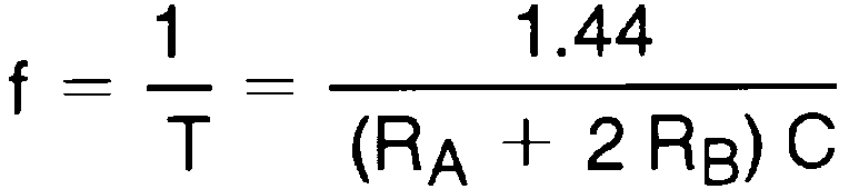
Figure 7-7 can be used for quick determination of these RC Values. The duty cycle, as a fraction of total period that the output is low, is:

Equation 5. GUID-565FC81F-733C-4351-978E-0F8A20B91620-low.gif
GUID-71024B69-B29C-47B6-88F0-AF3C60EC3B6E-low.pngFigure 7-7 Free-Running Frequency