SNOSC84D August 2012 – February 2015 LMH6882
PRODUCTION DATA.
- 1 Features
- 2 Applications
- 3 Description
- 4 Revision History
- 5 Pin Configuration and Functions
- 6 Specifications
- 7 Detailed Description
- 8 Application and Implementation
- 9 Power Supply Recommendations
- 10Layout
- 11Device and Documentation Support
- 12Mechanical, Packaging, and Orderable Information
Package Options
Refer to the PDF data sheet for device specific package drawings
Mechanical Data (Package|Pins)
- NJK|36
Thermal pad, mechanical data (Package|Pins)
Orderable Information
7 Detailed Description
7.1 Overview
The LMH6882 has been designed to replace traditional, fixed-gain amplifiers, as well as variable-gain amplifiers, with an easy-to-use device which can be flexibly configured to many different gain settings while maintaining excellent performance over the entire gain range. Many systems can benefit from this programmable-gain, DC-capable, differential amplifier. Last minute design changes can be implemented immediately, and external resistors are not required to set the gain. Gain control is enabled with a parallel- or a serial-control interface and as a result, the amplifier can also serve as a digitally controlled variable-gain amplifier (DVGA) for automatic gain control applications. Figure 50 and Figure 53 show typical implementations of the amplifier.
The LMH6882 is a fully differential amplifier optimized for signal path applications up to 1000 MHz. The LMH6882 has a 100-Ω input impedance and a low (less than 0.5 Ω) impedance output. The gain is digitally controlled over a 20 dB range from 26 dB to 6 dB. The LMH6882 is designed to replace fixed-gain differential amplifiers with a single, flexible-gain device. It has been designed to provide good noise figure and OIP3 over the entire gain range. This design feature is highlighted by the Dynamic Range Figure of merit (DRF). Traditional variable gain amplifiers generally have the best OIP3 and NF performance at maximum gain only.
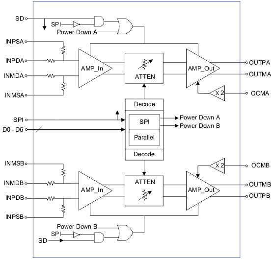
7.2 Functional Block Diagram
7.3 Feature Description
The LMH6882 has three functional stages, a low-noise amplifier, followed by a digital attenuator, and a low-distortion, low-impedance output amplifier. The amplifier has four signal input pins to accommodate both differential signals and single-ended signals. The amplifier has an OCM pin used to set the output common-mode voltage. There is a gain of 2 on this pin so that 1.25 V applied on that pin will place the output common mode at 2.5 V.
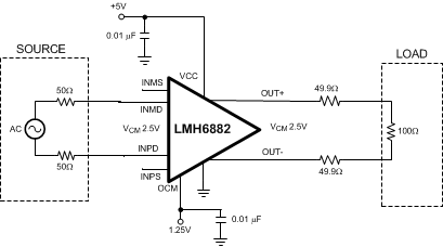 Figure 39. Typical Implementation With a Differential Input Signal
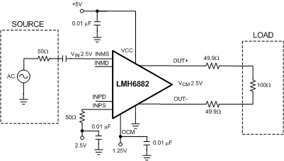 Figure 40. Typical Implementation With a Single-Ended Input Signal
7.4 Device Functional Modes
The LMH6882 will support two modes of control for its gain: a parallel mode and a serial mode (SPI compatible). Parallel mode is fastest and requires the most board space for logic line routing. Serial mode is compatible with existing SPI-compatible systems. The device has gain settings covering a range of 20 dB. In parallel mode, only 2-dB steps are available. The serial interface should be used for finer gain control of 0.25 dB for a gain between 6 dB and 26 dB of voltage gain. If fixed gain is desired, the digital pins can be strapped to ground or VCC, as required.
The device also supports two modes of power down control to enable power savings when the amplifier is not being used: using the SD pin (when SPI pin = Logic 0) and the power-down register (when SPI pin = Logic 1).
7.5 Programming
7.5.1 Digital Control of the Gain and Power-Down Pins
The LMH6882 was designed to interface with 2.5-V to 5-V CMOS logic circuits. If operation with 5-V logic is required care should be taken to avoid signal transients exceeding the amplifier supply voltage. Long, unterminated digital signal traces should be avoided. Signal voltages on the logic pins that exceed the device power-supply voltage may trigger ESD protection circuits and cause unreliable operation. Some digital input-output pins have different functions depending on the digital control mode. Table 1 shows the mapping of the digital pins. These functions for each pin will be described in the sections Parallel Interface and SPI-Compatible Serial Interface.
While the full gain range is available in parallel mode both channels must be set to the same gain. If independent channel control is desired, SPI mode must be used.
Table 1. Pins With Dual Functions
| PIN | SPI = 0 | SPI = 1 |
|---|---|---|
| 7 | D1 | SDI |
| 14 | D0 | SDO (1) |
| 8 | D2 | CLK |
| 9 | D3 | CS (active low) |
7.5.2 Parallel Interface
Parallel mode offers the fastest gain update capability with the drawback of requiring the most board space dedicated to control lines. To place the LMH6882 into parallel mode the SPI pin (pin 27) is set to the logical zero state. Alternately, the SPI pin can be connected directly to ground. The SPI pin has a weak internal resistor to ground. If left unconnected, the amplifier will operate in parallel mode.
In parallel mode the gain can be changed in 0.25-dB steps with a 7-bit gain control bus. The attenuator control pins are internally biased to logic high state with weak pull-up resistors, with the exception of D0 (pin 14) which is biased low due to the shared SDO function. If the control bus is left unconnected, the amplifier gain will be set to 6 dB. Table 2 shows the gain of the amplifier when controlled in parallel mode.
The LMH6882 has a 7-bit gain control bus. Data from the gain control pins is immediately sent to the gain circuit (that is, gain is changed immediately). To minimize gain change glitches all gain pins should change at the same time. Gain glitches could result from timing skew between the gain set bits. This is especially the case when a small gain change requires a change in state of three or more gain control pins. If necessary the PDA could be put into a disabled state while the gain pins are reconfigured and then brought active when they have settled.
Table 2. Gain Change Values for the Parallel-Gain Pins
| PIN | NAME | GAIN STEP SIZE (dB) |
|---|---|---|
| 14 | D0 | 0.25 |
| 7 | D1 | 0.5 |
| 8 | D2 | 1 |
| 9 | D3 | 2 |
| 21 | D4 | 4 |
| 20 | D5 | 8 |
| 19 | D6 | 16 |
| Gain combinations that exceed 80 will result in minimum gain of 6 dB. | ||
Table 3. Amplifier Gain for Selected Control Pin Combinations
| CONTROL PINS LOGICAL LEVEL IN PARALLEL MODE. (X = DON'T CARE) | GAIN = 26 - 0.25 × DECIMAL VALUE AND GAIN ≥ 6 dB | |||||||
|---|---|---|---|---|---|---|---|---|
| D6 | D5 | D4 | D3 | D2 | D1 | D0 | Decimal/Hex Value | Amplifier Voltage Gain (dB) |
| 0 | 0 | 0 | 0 | 0 | 0 | 0 | 0 / 0 | 26 |
| 0 | 0 | 0 | 0 | 0 | 0 | 1 | 1 / 1 | 25.75 |
| 0 | 0 | 0 | 0 | 0 | 1 | 0 | 2 / 2 | 25.5 |
| 0 | 0 | 0 | 0 | 0 | 1 | 1 | 3 / 3 | 25.25 |
| 0 | 0 | 0 | 0 | 1 | 0 | 0 | 4 / 4 | 25 |
| 0 | 0 | 0 | 0 | 1 | 0 | 1 | 5 / 5 | 24.75 |
| 0 | 0 | 0 | 0 | 1 | 1 | 0 | 6 / 5 | 24.5 |
| 0 | 0 | 0 | 0 | 1 | 1 | 1 | 7 / 7 | 24.25 |
| 0 | 0 | 0 | 1 | 0 | 0 | 0 | 8 / 8 | 24 |
| 0 | 0 | 1 | 0 | 0 | 0 | 0 | 16 / 10 | 22 |
| 0 | 0 | 1 | 1 | 0 | 0 | 0 | 24 / 18 | 20 |
| 0 | 1 | 0 | 0 | 0 | 0 | 0 | 32 / 20 | 18 |
| 0 | 1 | 0 | 1 | 0 | 0 | 0 | 40 / 28 | 16 |
| 0 | 1 | 1 | 0 | 0 | 0 | 0 | 48 / 30 | 14 |
| 0 | 1 | 1 | 1 | 0 | 0 | 0 | 56 / 38 | 12 |
| 1 | 0 | 0 | 0 | 0 | 0 | 0 | 64 / 40 | 10 |
| 1 | 0 | 0 | 1 | 0 | 0 | 0 | 72 / 48 | 8 |
| 1 | 0 | 1 | 0 | 0 | 0 | 0 | 80 / 50 | 6 |
| 1 | 0 | 1 | X | X | X | X | > 80 / 50 | 6 |
| 1 | 1 | X | X | X | X | X | > 80 / 50 | 6 |
For fixed-gain applications the attenuator control pins should be connected to the desired logic state instead of relying on the weak internal bias. Data from the gain-control pins directly drive the amplifier gain circuits. To minimize gain change glitches all gain pins should be driven with minimal skew. If gain-pin timing is uncertain, undesirable transients can be avoided by using the shutdown pin to disable the amplifier while the gain is changed. Gain glitches are most likely to occur when multiple bits change value for a small gain change, such as the gain change from 10 dB to 12 dB which requires changing all 4 gain control pins.
A shutdown pin (SD == 0, amplifier on, SD == 1, amplifier off) is provided to reduce power consumption by disabling the highest power portions of the amplifier. The digital control circuit is not shut down and will preserve the last active gain setting during the disabled state. See the Typical Characteristics section for disable and enable timing information. The SD pin is functional in parallel mode only and disabled in serial mode.
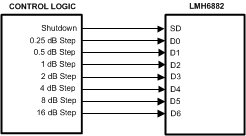 Figure 41. Parallel Mode Connection
7.5.3 SPI-Compatible Serial Interface
The serial interface allows a great deal of flexibility in gain programming and reduced board complexity. The LMH6882 serial interface is a generic 4-wire synchronous interface compatible with SPI type interfaces that are used on many microcontrollers and DSP controllers. Using only 4 wires, the SPI mode offers access to the 0.25-dB gain steps of the amplifier.
For systems where gain is changed only infrequently, or where only slower gain changes are required, serial mode is the best choice. To place the LMH6882 into serial mode the SPI pin (Pin 27) should be put into the logic high state. Alternatively the SPI pin can be connected directly to the 5-V supply bus. In this configuration the pins function as shown in Table 2. The SPI interface uses the following signals: clock input (CLK); serial data in (SDI); serial data out (SDO); and serial chip select (CS). The chip-select pin is active low meaning the device is selected when the pin is low.
The SD pin is inactive in the serial mode. This pin can be left disconnected for serial mode. The SPI interface has the ability to shutdown the amplifier without using the SD pin.
The CLK pin is the serial clock pin. It is used to register the input data that is presented on the SDI pin on the rising edge and to source the output data on the SDO pin on the falling edge. The user may disable clock and hold it in the low state, as long as the clock pulse-width minimum specification is not violated when the clock is enabled or disabled. The clock pulse-width minimum is equal to one setup plus one hold time, or 6 ns.
The CS pin is the chip-select pin. This pin is active low; the chip is selected in the logic low state. Each assertion starts a new register access - i.e., the SDATA field protocol is required. The user is required to de-assert this signal after the 16th clock. If the CS pin is de-asserted before the 16th clock, no address or data write will occur. The rising edge captures the address just shifted in and, in the case of a write operation, writes the addressed register. There is a minimum pulse-width requirement for the deasserted pulse - which is specified in the Electrical Characteristics section.
The SDI pin is the input pin for the serial data. It must observe setup / hold requirements with respect to the SCLK. Values can be found in the Electrical Characteristics table (refer to electrical table of the DS). Each write cycle is 16-bit long.
The SDO pin is the data output pin. This output is normally at a high-impedance state, and is driven only when CS is asserted. Upon CS assertion, contents of the register addressed during the first byte are shifted out with the second 8 SCLK falling edges. The SDO pin is a current output and requires external bias resistor to develop the correct logic voltage. See Figure 43 for details on sizing the external bias resistor. Resistor values of 180 Ω to 400 Ω are recommended. The SDO pin can source 10 mA in the logic high state. With a bias resistor of 250 Ω the logic 1 voltage would be 2.5 V. In the logic 0 state, the SDO output is off, and no current flows, so the bias resistor will pull the voltage to 0 V.
Each serial interface access cycle is exactly 16 bits long as shown in Figure 42. Each signal's function is described below. the read timing is shown in Figure 44.
The external bias resistor means that in the high impedance state the SDO pin impedance is equal to the external bias resistor value. If bussing multiple SPI devices make sure that the SDO pins of the other devices can drive the bias resistor.
The serial interface has 6 registers with address [0] to address [6]. Table 4 shows the content of each SPI register. Registers 0 and 1 are read only. Registers 2 through 6 are read/write and control the gain and power of the amplifier. Register contents and functions are detailed below.
Table 4. SPI Registers by Address and Function
| Address | R/W | Name | Default Value Hex (Dec) |
|---|---|---|---|
| 0 | R | Revision ID | 1 (1) |
| 1 | R | Product ID | 21 (33) |
| 2 | R/W | Power Control | 0 (0) |
| 3 | R/W | Attenuation A | 50 (80) |
| 4 | R/W | Attenuation B | 50 (80) |
| 5 | R/W | Channel Control | 3 (3) |
Table 5. Serial Word Format for Register 2: Power Control
| 7 | 6 | 5 | 4 | 3 | 2 | 1 | 0 |
|---|---|---|---|---|---|---|---|
| RES | RES | CHA1 | CHB1 | CHA2 | CHB2 | RES | RES |
| CHA1 and CHA2 = 0 for ON, CHA1 and CHA2 = 1 for OFF | |||||||
| CHB1 and CHB2 = 0 for ON, CHB1 and CHB2 = 1 for OFF | |||||||
Table 6. Serial Word Format for Registers 3, 4: Gain Control
| 7 | 6 | 5 | 4 | 3 | 2 | 1 | 0 |
|---|---|---|---|---|---|---|---|
| RES | Gain = 26 — (register value * 0.25) valid range is 0 to 80 | ||||||
Table 7. Serial Word Format for Register 5: Channel Control
| 7 | 6 | 5 | 4 | 3 | 2 | 1 | 1 |
|---|---|---|---|---|---|---|---|
| RES | SYNC | Load A | Load B | ||||
The Channel Control register controls how registers 3 and 4 work. When the SYNC bit is set to 1 both channel A and channel B are set to the gain indicated in register 3. When the SYNC bit is set to zero, register 3 controls channel A, and register 4 controls channel B. When the Load A bit is zero data written to register 3 does not transfer to channel A. When the Load A bit is set to 1 the gain of channel A is set equal to the value indicated in register 3. The Load B bit works the same for channel B and register 4.
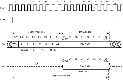 Figure 42. Serial Interface Protocol (SPI Compatible)
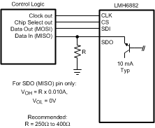 Figure 43. Internal Operation of the SDO Pin
| R/Wb | Read / Write bit. A value of 1 indicates a read operation, while a value of 0 indicates a write operation. |
| Reserved | Not used. Must be set to 0. |
| ADDR: | Address of register to be read or written. |
| DATA | In a write operation the value of this field will be written to the addressed register when the chip-select pin is deasserted. In a read operation this field is ignored. |
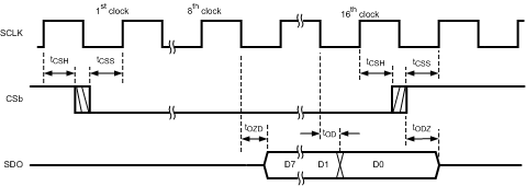 Figure 44. Read Timing