SNOSC84D August 2012 – February 2015 LMH6882
PRODUCTION DATA.
- 1 Features
- 2 Applications
- 3 Description
- 4 Revision History
- 5 Pin Configuration and Functions
- 6 Specifications
- 7 Detailed Description
- 8 Application and Implementation
- 9 Power Supply Recommendations
- 10Layout
- 11Device and Documentation Support
- 12Mechanical, Packaging, and Orderable Information
Package Options
Refer to the PDF data sheet for device specific package drawings
Mechanical Data (Package|Pins)
- NJK|36
Thermal pad, mechanical data (Package|Pins)
Orderable Information
6 Specifications
6.1 Absolute Maximum Ratings(1)(2)
| MIN | MAX | UNIT | |
|---|---|---|---|
| Positive supply voltage (VCC) | −0.6 | 5.5 | V |
| Differential voltage between any two grounds | < 200 | mV | |
| Analog input voltage | −0.6 | 5.5 | V |
| Digital input voltage | −0.6 | 5.5 | V |
| Output short circuit duration (one pin to ground) | Infinite | ||
| Junction temperature | +150 | °C | |
| Soldering information: infrared or convection (30 sec) | 260 | °C | |
| Storage temperature, Tstg | −65 | 150 | °C |
(1) Stresses beyond those listed under Absolute Maximum Ratings may cause permanent damage to the device. These are stress ratings only, which do not imply functional operation of the device at these or any other conditions beyond those indicated under Recommended Operating Conditions. Exposure to absolute-maximum-rated conditions for extended periods may affect device reliability.
(2) If Military/Aerospace specified devices are required, please contact the Texas Instruments Sales Office/Distributors for availability and specifications.
6.2 ESD Ratings
| VALUE | UNIT | |||
|---|---|---|---|---|
| V(ESD) | Electrostatic discharge | Human body model (HBM), per ANSI/ESDA/JEDEC JS-001(1) | ±1000 | V |
| Charged-device model (CDM), per JEDEC specification JESD22-C101(2) | ±250 | |||
(1) JEDEC document JEP155 states that 500-V HBM allows safe manufacturing with a standard ESD control process.
(2) JEDEC document JEP157 states that 250-V CDM allows safe manufacturing with a standard ESD control process.
6.3 Recommended Operating Conditions
over operating free-air temperature range (unless otherwise noted)| MIN | MAX | UNIT | |
|---|---|---|---|
| Supply voltage (VCC) | 4.75 | 5.25 | V |
| Differential voltage between any two grounds | < 10 | mV | |
| Analog input voltage, AC coupled |
0 | VCC | V |
| Temperature range (1) | –40 | 85 | °C |
6.4 Thermal Information
| THERMAL METRIC(1) | LMH6882 | UNIT | |
|---|---|---|---|
| NJK (WQFN) | |||
| 36 PINS | |||
| RθJA | Junction-to-ambient thermal resistance | 33.6 | °C/W |
| RθJC(top) | Junction-to-case (top) thermal resistance | 16.9 | |
| RθJB | Junction-to-board thermal resistance | 7.8 | |
| ψJT | Junction-to-top characterization parameter | 0.3 | |
| ψJB | Junction-to-board characterization parameter | 7.7 | |
| RθJC(bot) | Junction-to-case (bottom) thermal resistance | 3.5 | |
(1) For more information about traditional and new thermal metrics, see the IC Package Thermal Metrics application report, SPRA953.
6.5 Electrical Characteristics
The following specifications apply for single supply with VCC = 5 V, Maximum Gain (26 dB), RL = 200 Ω.(2)(5)(6)| TEST CONDITIONS | MIN(4) | TYP(3) | MAX(4) | UNIT | ||
|---|---|---|---|---|---|---|
| DYNAMIC PERFORMANCE | ||||||
| 3dBBW | −3-dB Bandwidth | VOUT = 2 VPPD | 2.4 | GHz | ||
| NF | Noise Figure | Source Resistance (Rs) = 100 Ω | 9.7 | dB | ||
| OIP3 | Output Third Order Intercept Point(9) | f = 100 MHz, POUT = 4 dBm per tone, tone spacing = 1 MHz | 42 | dBm | ||
| f = 200 MHz, POUT = 4 dBm per tone, tone spacing = 2 MHz | 40 | |||||
| OIP2 | Output Second Order Intercept Point | POUT= 4 dBm per Tone, f1 = 112.5 MHz, f2=187.5 MHz | 76 | dBm | ||
| IMD3 | Third Order Intermodulation Products | f = 100 MHz, VOUT = 4 dBm per tone, tone spacing = 1 MHz | −76 | dBc | ||
| f = 200 MHz, POUT = 4 dBm per tone, tone spacing = 2 MHz | −72 | |||||
| P1dB | 1-dB Compression Point | Output power | 17 | dBm | ||
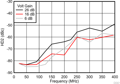
| HD2 | Second Order Harmonic Distortion | f = 200 MHz, VOUT = 4 dBm | −70 | dBc | ||
| HD3 | Third Order Harmonic Distortion | f = 200 MHz, POUT = 4 dBm | −76 | dBc | ||
| CMRR | Common Mode Rejection Ratio (8) | Pin = −15 dBm, f = 100 MHz | −40 | dBc | ||
| SR | Slew Rate | 6000 | V/us | |||
| Output Voltage Noise | Maximum Gain f > 1 MHz | 47 | nV/√Hz | |||
| Input Referred Voltage Noise | Maximum Gain f > 1 MHz | 2.3 | nV/√Hz | |||
| ANALOG I/O | ||||||
| RIN | Input Resistance | Differential, INPD to INMD | 100 | Ω | ||
| RIN | Input Resistance | Single Ended, INPS or INMS, 50-Ω termination on unused input | 50 | Ω | ||
| VICM | Input Common Mode Voltage | Self Biased | 2.5 | V | ||
| Maximum Input Voltage Swing | Volts peak to peak, differential | 2 | VPPD | |||
| Maximum Differential Output Voltage Swing | Differential, f < 10 MHz | 6 | VPPD | |||
| ROUT | Output Resistance | Differential, f = 100 MHz | 0.4 | Ω | ||
| GAIN PARAMETERS | ||||||
| Maximum Voltage Gain | Parallel Inputs (INPD and INMD), Rs = 100 Ω | 26 | dB | |||
| Single ended input (INMS or INPS), 50 Ω Rs and 50 Ω termination on unused input. | 26.6 | |||||
| Minimum Gain | Gain Code = 80d or 50h | 6 | dB | |||
| Gain Steps | 80 | |||||
| Gain Step Size | 0.25 | dB | ||||
| Gain Step Error | Any two adjacent steps over entire range | ±0.125 | dB | |||
| Gain Step Phase Shift | Any two adjacent steps over entire range | ±3 | Degrees | |||
| Channel to Channel Gain Matching | f = 100 MHz, over entire gain range | 0.2 | dB | |||
| Channel to Channel Phase Matching | f= 100 MHz, over entire gain range | 1.5 | Degrees | |||
| Gain Step Switching Time | 20 | ns | ||||
| Enable/ Disable Time | Settled to 90% level | 15 | ns | |||
| POWER REQUIREMENTS | ||||||
| ICC | Supply Current | 200 | 270 | mA | ||
| P | Power | 1 | W | |||
| ICC | Disabled Supply Current | 25 | mA | |||
| ALL DIGITAL INPUTS | ||||||
| Logic Compatibility | TTL, 2.5 V CMOS, 3.3 V CMOS, 5 V CMOS | |||||
| VIL | Logic Input Low Voltage | 0.4 | V | |||
| VIH | Logic Input High Voltage | 2.0-5.0 | V | |||
| IIH | Logic Input High Input Current | −9 | μA | |||
| IIL | Logic Input Low Input Current | −47 | μA | |||
| PARALLEL MODE TIMING | ||||||
| tGS | Setup Time | 3 | ns | |||
| tGH | Hold Time | 3 | ns | |||
| SERIAL MODE | ||||||
| fCLK | SPI Clock Frequency | 50% duty cycle, ATE tested @ 10 MHz | 10 | 50 | MHz | |
(1) The maximum power dissipation is a function of TJ(MAX), θJA and the ambient temperature TA. The maximum allowable power dissipation at any ambient temperature is PD = (TJ(MAX) – TA)/ θJA. All numbers apply for packages soldered directly onto a PC Board.
(2) Electrical Table values apply only for factory testing conditions at the temperature indicated. No specification of parametric performance is indicated in the electrical tables under conditions different than those tested
(3) Typical values represent the most likely parametric norm as determined at the time of characterization. Actual typical values may vary over time and will also depend on the application and configuration. The typical values are not tested and are not ensured on shipped production material.
(4) Limits are 100% production tested at 25°C. Limits over the operating temperature range are specified through correlation using Statistical Quality Control (SQC) methods.
(5) Negative input current implies current flowing out of the device.
(6) Drift determined by dividing the change in parameter at temperature extremes by the total temperature change.
(7) LMH6881 devices have been used for some typical performance plots.
(8) CMRR is defined as the differential response at the output in response to a common mode signal at the input.
(9) OIP3 is the third order intermodulation intercept point. In this data sheet OIP3 numbers are single power measurements where OIP3 = IMD3 / 2 + POUT (per tone). OIP2 is the second order intercept point where OIP2 = IMD2 + POUT (per tone). HD2 is the second order harmonic distortion and is a single tone measurement. HD3 is the third order harmonic distortion and is a single tone measurement. Power measurements are made at the amplifier output pins.
6.6 Typical Characteristics
(Unless otherwise specified, the following conditions apply: TA = 25°C, VCC = 5 V, RL = 200 Ω, Maximum Gain, Differential Input.)(7)
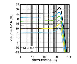 Figure 1. Frequency Response Over Gain Range
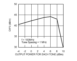 Figure 3. OIP3 vs Output Power
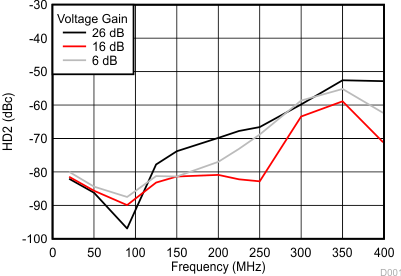
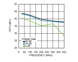 Figure 5. OIP3 vs Frequency
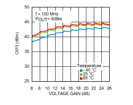 Figure 7. OIP3 vs Temperature
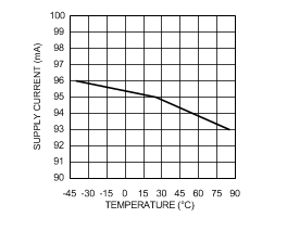 Figure 9. Supply Current vs Temperature
| Pout = 4 dBm |
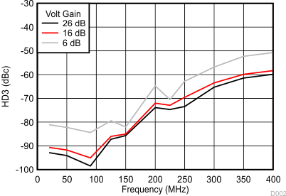
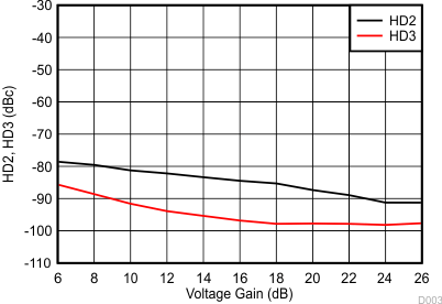
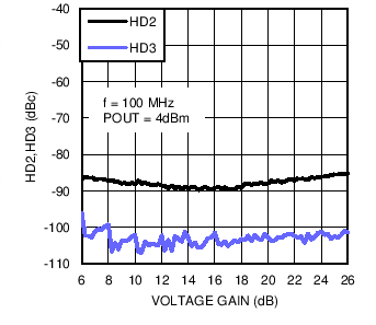 Figure 13. HD2 & HD3 vs Voltage Gain
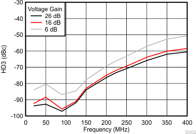
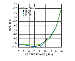 Figure 15. HD3 vs Output Power
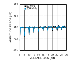 Figure 17. Gain Step Amplitude Error
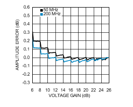 Figure 19. Cumulative Amplitude Error
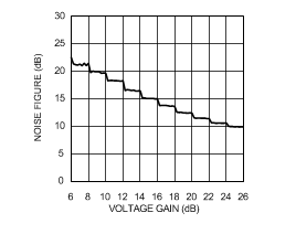 Figure 21. Noise Figure vs Voltage Gain
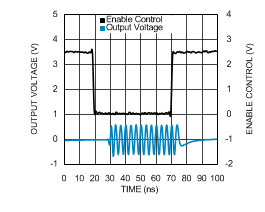 Figure 23. Channel Enable Control Timing Behavior
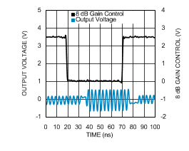 Figure 25. 8-dB Gain Control Timing Behavior
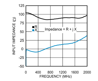 Figure 27. Differential Input Impedance
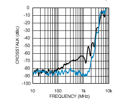 Figure 29. Crosstalk
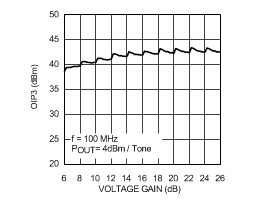 Figure 31. OIP3 Overvoltage Gain Range
Figure 2. OIP3 vs Voltage Gain
Figure 31. OIP3 Overvoltage Gain Range
Figure 2. OIP3 vs Voltage Gain
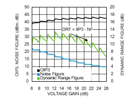 Figure 4. Dynamic Range Figure vs Voltage Gain
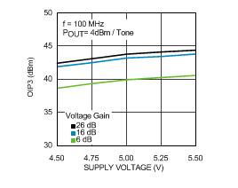 Figure 6. OIP3 vs Supply Voltage
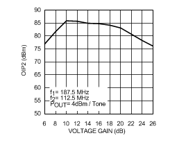 Figure 8. OIP2 vs Voltage Gain
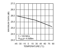 Figure 10. Maximum Gain vs Temperature
| Pout = 4 dBm |
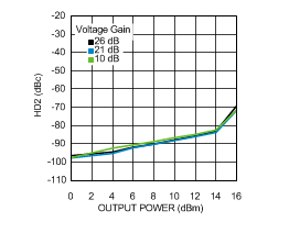 Figure 14. HD2 vs Output Power
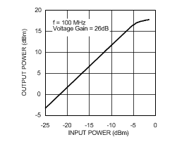 Figure 16. Output Power vs Input Power
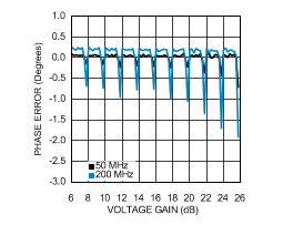 Figure 18. Gain Step Phase Error
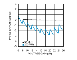 Figure 20. Cumulative Phase Error
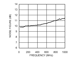 Figure 22. Noise Figure vs Frequency
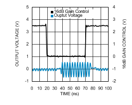 Figure 24. 16-dB Gain Control Timing Behavior
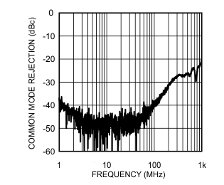 Figure 26. Common Mode Rejection (Sdc21) vs Frequency
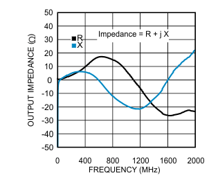 Figure 28. Differential Output Impedance
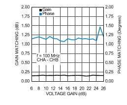 Figure 30. Channel A to Channel B Gain and Phase Matching
Figure 32. Channel A to Channel B Gain and Phase Matching
Figure 30. Channel A to Channel B Gain and Phase Matching
Figure 32. Channel A to Channel B Gain and Phase Matching
6.6.1 Single-Ended Input
(Unless otherwise specified, the following conditions apply: TA = 25°C, VCC = 5 V, RL = 200Ω, Maximum Gain, Differential Input).
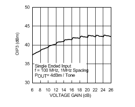 Figure 33. OIP3 vs Voltage Gain
| Pout = 4 dBm |
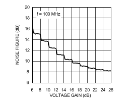 Figure 37. Noise Figure vs Voltage Gain
| Pout = 4 dBm | ||
| f = 100 MHz | Pout = 4 dBm |
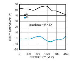 Figure 38. Input Impedance