SNAS634B March 2014 – January 2016 LMP92066
PRODUCTION DATA.
- 1 Features
- 2 Applications
- 3 Description
- 4 Simplified Schematic
- 5 Revision History
- 6 Pin Configuration and Functions
- 7 Specifications
-
8 Detailed Description
- 8.1 Overview
- 8.2 Functional Block Diagram
- 8.3 Features Description
- 8.4 Device Functional Modes
- 8.5
Programming
- 8.5.1 Temperature Sensor Output Data Access Registers
- 8.5.2 DAC Input Data Registers
- 8.5.3 Temperature Sensor Status Register
- 8.5.4 Override Control Register
- 8.5.5 Override Data Registers
- 8.5.6 EEPROM Control Register
- 8.5.7 Software RESET Register
- 8.5.8 Access Control Register
- 8.5.9 Block I2C Access Control Register
- 8.5.10 I2C Address LOCK Register
- 8.5.11 Output Drive Supply Status Register
- 8.5.12 Device Version Register
- 8.5.13 EEPROM Burn Counter
- 8.5.14 LUT Coefficient Registers
- 8.5.15 LUT Control Registers
- 8.5.16 Notepad Registers
- 8.6 Register Map
- 9 Application and Implementation
- 10Power Supply Recommendations
- 11Layout
- 12Device and Documentation Support
- 13Mechanical, Packaging, and Orderable Information
Package Options
Mechanical Data (Package|Pins)
- PWP|16
Thermal pad, mechanical data (Package|Pins)
- PWP|16
Orderable Information
10 Power Supply Recommendations
The device rails VIO, VDD, and VDDB (VSSB in GaN mode) should be supplied from a well-regulated power supply capable of sourcing at least 50 mA. The required supply levels are shown in the Specifications tables of this document. Along with ceramic bypass capacitors, additional bulk capacitance is recommended on the VDD node. The function of this bulk capacitance is to provide the momentary increases in the supply current requirements due to the EEPROM activity. An electrolytic capacitor with a value of 10 μF to 47 μF is a typical choice.
10.1 VDD Supply Sourcing
The power supply powering the VDD pin must be capable of sourcing a minimum of 50mA. This is required in order to avoid the continuous activation of the LMP92066’s power-on-reset (POR) circuit. When the VDD supply rail passes through the POR voltage of approximately 4.2V (either rising or falling edge), an increase in supply current occurs. If the power supply is not capable of sourcing the 50mA that is required under worst case conditions, the voltage supplied to VDD will not increase beyond the POR voltage level and the LMP92066’s POR circuitry remains active and continues to draw excess current. This excess current draw is approximately 20mA under nominal conditions.
Since the LMP92066’s POR circuitry also responds to the discharge (falling edge) of the supply line, an increase in supply current occurs when the VDD supply is turned off as well. Similar to the condition described above, if the VDD supply is not capable of sourcing a minimum of 50mA, an increase in VDD supply current can be experienced if the VDD supply is immediately ramped back up after being discharged. Under this circumstance, the increase in VDD supply current will persist until the voltage surpasses 4.2V. This is a result of the POR circuitry never turning off. The POR circuit will only turn off once the VDD supply has passed through the POR voltage level of 4.2V.
10.2 IVDD During EEPROM BURN
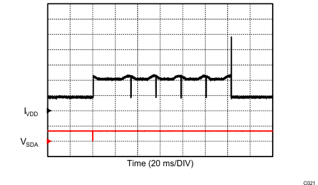
Figure 51 shows the transient behavior of IVDD due to the EEPROM BURN operation. VSDA trace activity is used as the trigger. The triggering event is the BURN command sent via the I2C interface. During the BURN the IVDD increases to almost 4 mA for 125 ms. The 10-mA peaking in IVDD is due to the TRANSFER of newly stored data from EEPROM back to the operating memory – this is part of the internal error detection and correction process.

| IVDD = 2mA/div | VSDA = 5V/div | |
10.3 IVDD During EEPROM TRANSFER
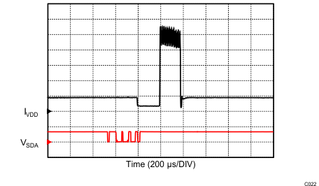
The transfer of data, from the EEPROM to the operating memory, results in the temporary increase in supply current IVDD. The total IVDD increases to about 10 mA for the duration of the TRANFER operation, typically 200 µs. Given the infrequent occurrence, and the short duration, the increased IVDD can be easily supplied by the external bulk capacitors; that is, this does not represent an additional burden to the system power supply. The typical IVDD transient during TRANSFER is shown in Figure 52. The triggering event is the TRANSFER command issued via the I2C interface.

| IVDD = 2mA/div | VSDA = 5V/div | |
The TRANSFER operation occurs due to the following:
- Power-On RESET
- Software RESET
- EEPROM TRANSFER command issued via the I2C interface
- Upon completion of the EEPROM BURN operation, as a data verification step.