SNVS817B June   2012  – June 2019 LMR12015 , LMR12020

PRODUCTION DATA.  

  1. Features
  2. Applications
  3. Description
    1.     Device Images
      1.      Typical Application Circuit
  4. Revision History
  5. Pin Configuration and Functions
    1.     Pin Descriptions
  6. Specifications
    1. 6.1 Absolute Maximum Ratings
    2. 6.2 Recommended Operating Ratings
    3. 6.3 Electrical Characteristics
    4. 6.4 Typical Performance Characteristics
  7. Detailed Description
    1. 7.1 Overview
    2. 7.2 Functional Block Diagram
    3. 7.3 Feature Description
      1. 7.3.1  Boost Function
      2. 7.3.2  Low Input Voltage Considerations
      3. 7.3.3  High Output Voltage Considerations
      4. 7.3.4  Frequency Synchronization
      5. 7.3.5  Current Limit
      6. 7.3.6  Frequency Foldback
      7. 7.3.7  Soft Start
      8. 7.3.8  Output Overvoltage Protection
      9. 7.3.9  Undervoltage Lockout
      10. 7.3.10 Thermal Shutdown
    4. 7.4 Device Operation Modes
      1. 7.4.1 Enable Pin / Shutdown Mode
  8. Application and Implementation
    1. 8.1 Application Information
    2. 8.2 Typical Application
      1. 8.2.1 Detailed Design Procedure
        1. 8.2.1.1  Custom Design With WEBENCH® Tools
        2. 8.2.1.2  Inductor Selection
          1. 8.2.1.2.1 Inductor Calculation Example
          2. 8.2.1.2.2 Inductor Material Selection
        3. 8.2.1.3  Input Capacitor
        4. 8.2.1.4  Output Capacitor
        5. 8.2.1.5  Catch Diode
        6. 8.2.1.6  Boost Diode (Optional)
        7. 8.2.1.7  Boost Capacitor
        8. 8.2.1.8  Output Voltage
        9. 8.2.1.9  Feedforward Capacitor (Optional)
        10. 8.2.1.10 Calculating Efficiency and Junction Temperature
          1. 8.2.1.10.1 Schottky Diode Conduction Losses
          2. 8.2.1.10.2 Inductor Conduction Losses
          3. 8.2.1.10.3 MOSFET Conduction Losses
          4. 8.2.1.10.4 MOSFET Switching Losses
          5. 8.2.1.10.5 IC Quiescent Losses
          6. 8.2.1.10.6 MOSFET Driver Losses
          7. 8.2.1.10.7 Total Power Losses
          8. 8.2.1.10.8 Efficiency Calculation Example
          9. 8.2.1.10.9 Calculating the LMR2015/20 Junction Temperature
      2. 8.2.2 Application Curves
      3. 8.2.3 LMR12015/20 Circuit Examples
  9. Layout
    1. 9.1 Layout Considerations
      1. 9.1.1 Compact Layout
      2. 9.1.2 Ground Plane and Shape Routing
      3. 9.1.3 FB Loop
      4. 9.1.4 PCB Summary
  10. 10Device and Documentation Support
    1. 10.1 Device Support
      1. 10.1.1 Third-Party Products Disclaimer
      2. 10.1.2 Development Support
        1. 10.1.2.1 Custom Design With WEBENCH® Tools
    2. 10.2 Related Links
    3. 10.3 Receiving Notification of Documentation Updates
    4. 10.4 Community Resources
    5. 10.5 Trademarks
    6. 10.6 Electrostatic Discharge Caution
    7. 10.7 Glossary
  11. 11Mechanical, Packaging, and Orderable Information

Package Options

Mechanical Data (Package|Pins)
Thermal pad, mechanical data (Package|Pins)
Orderable Information

Typical Performance Characteristics

All curves taken at VIN = 12 V, VBOOST – VSW = 4.3 V and TA = 25°C, unless specified otherwise.
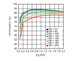
LMR12015 LMR12020 301970b6.gif
VIN = 5 V ƒSW = 2 MHz
Refer To Figure 37
Figure 1. Efficiency vs Load Current
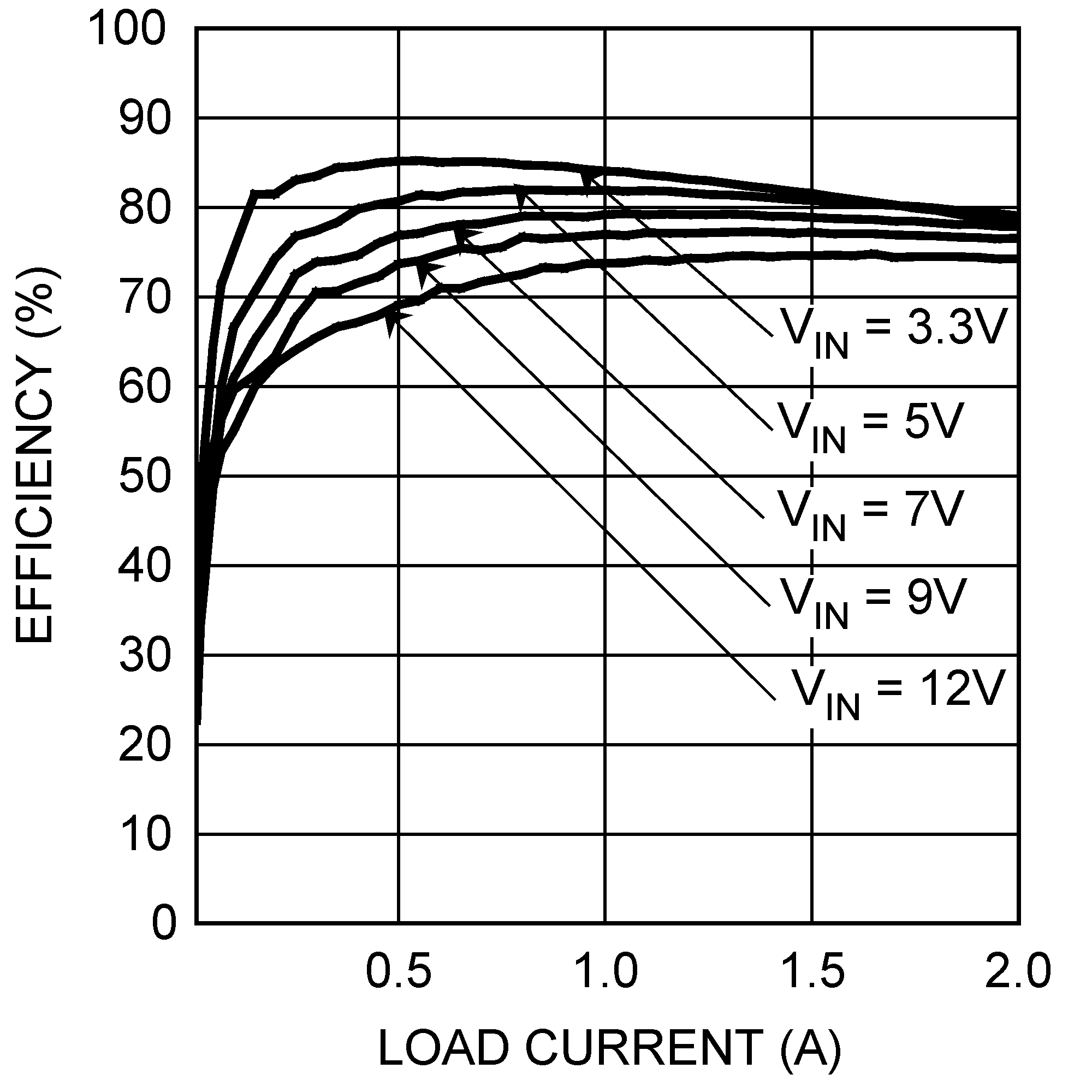
LMR12015 LMR12020 30197084.png
VOUT = 1.8 V ƒSW = 2 MHz
Refer To Figure 40
Figure 3. Efficiency vs Load Current
LMR12015 LMR12020 301970b1.png
Figure 5. Short Circuit Release
LMR12015 LMR12020 30197054.png
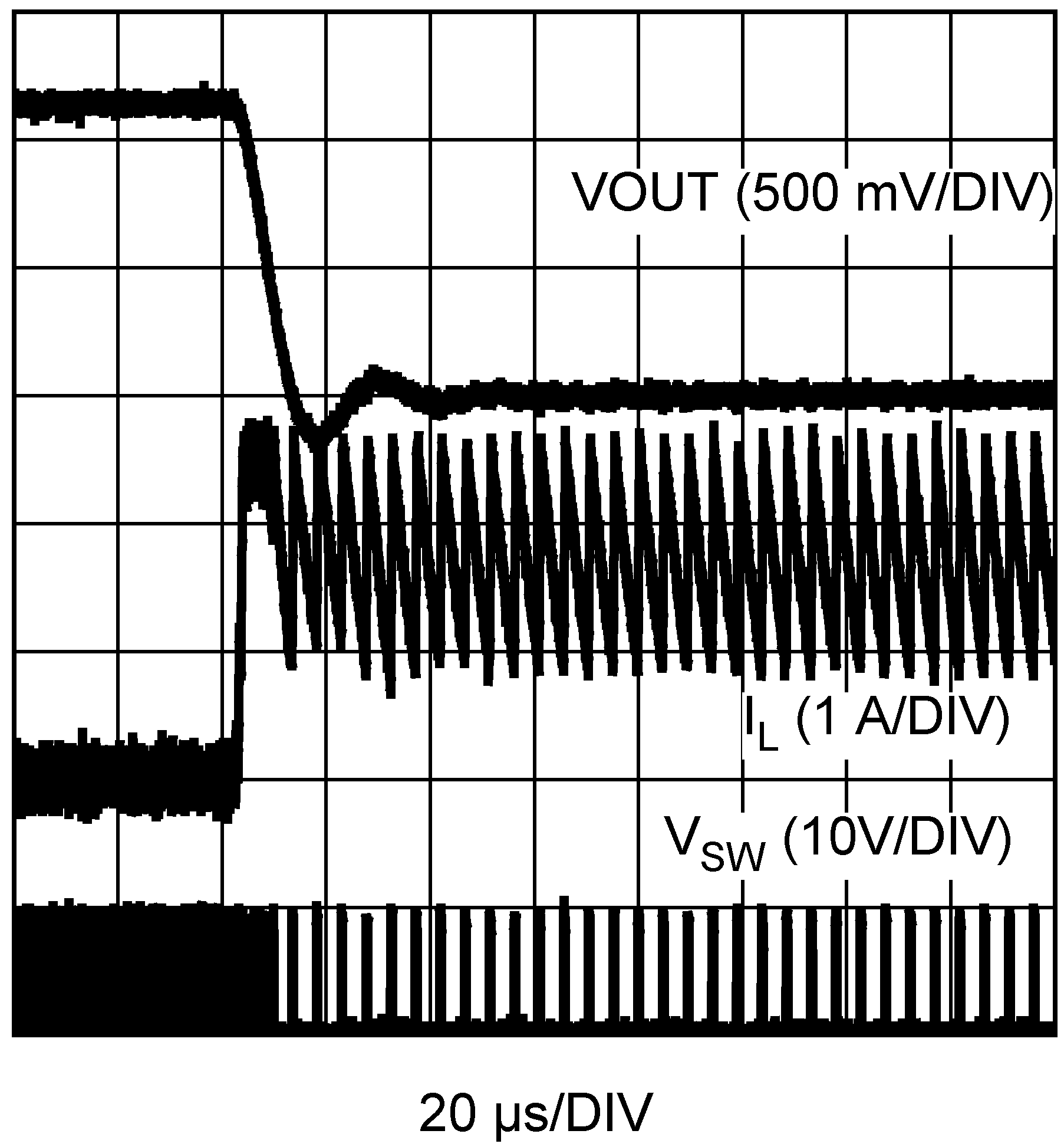
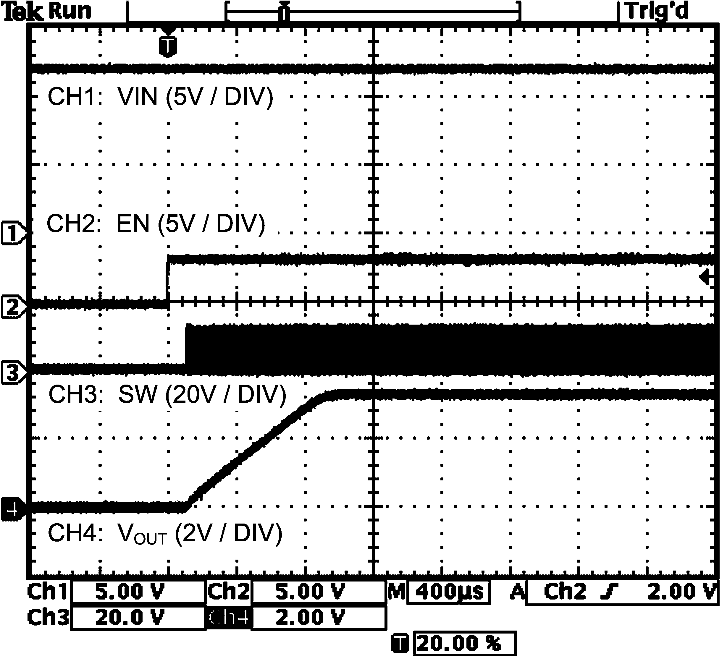
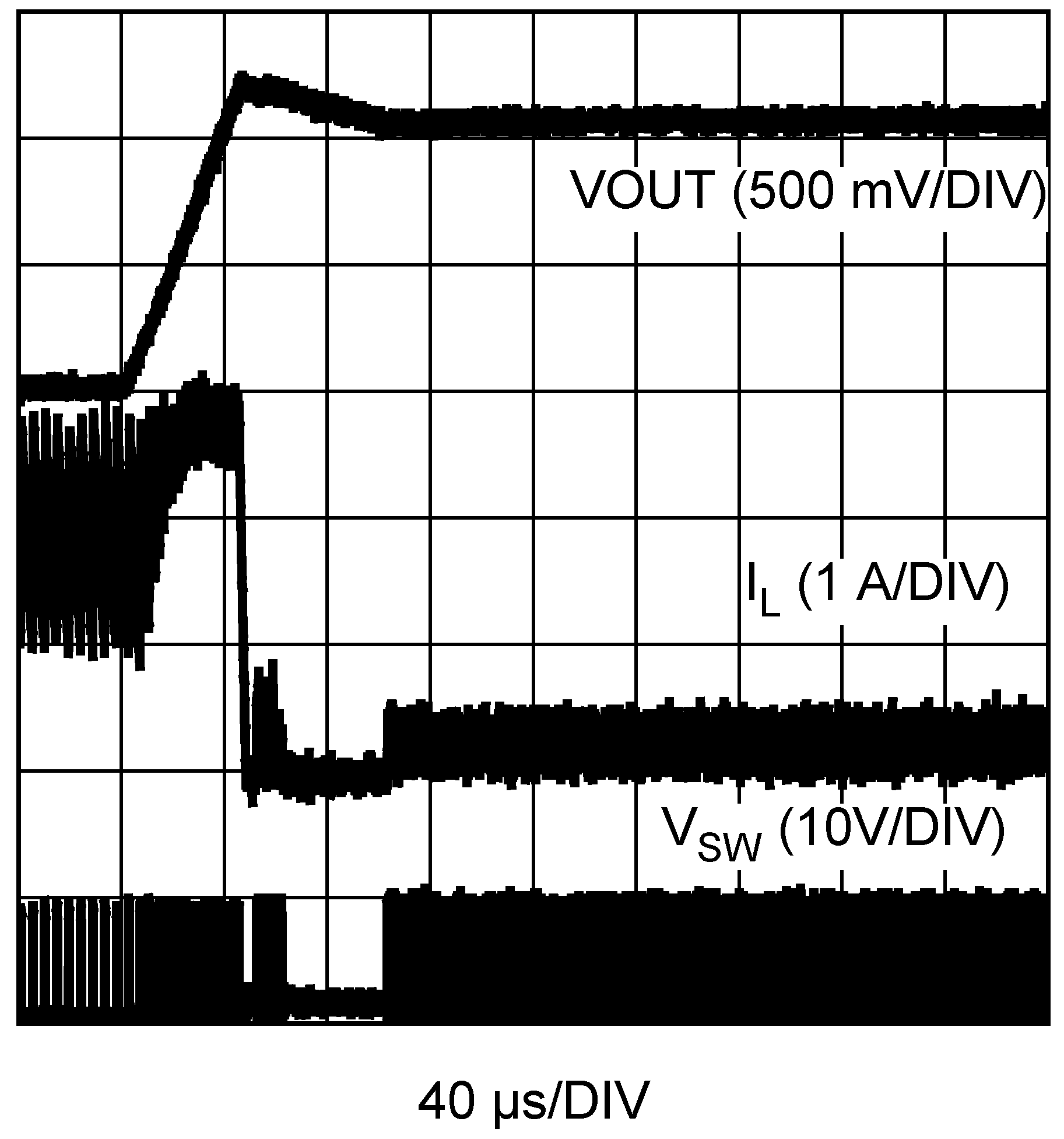
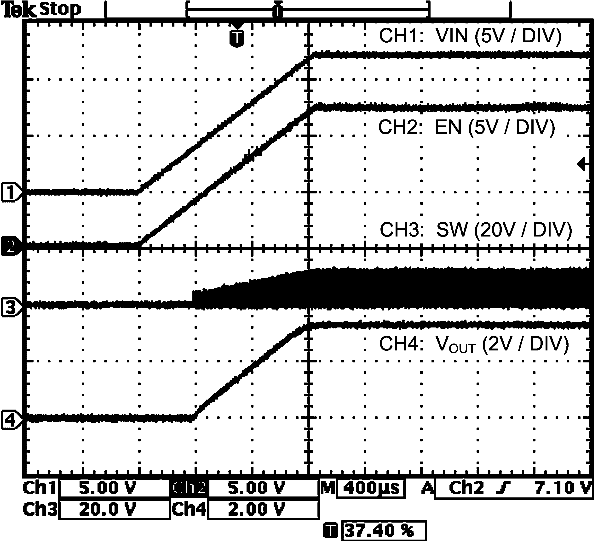
Figure 7. Soft Start With EN Tied To VIN
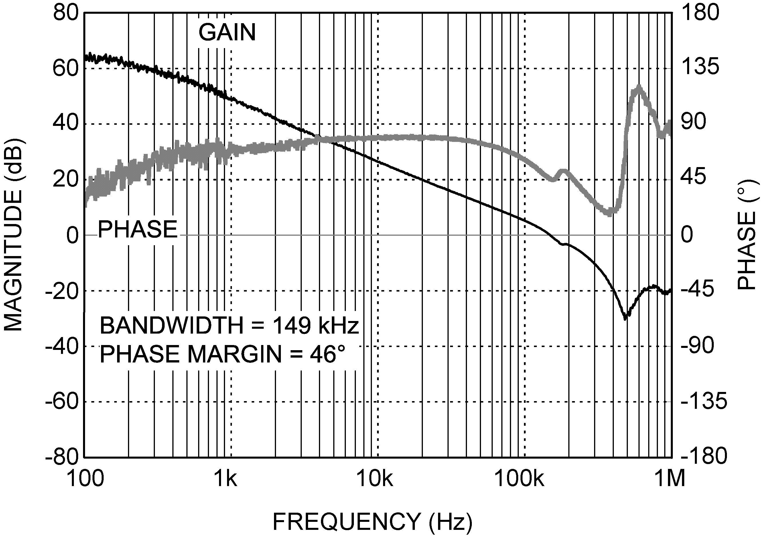
LMR12015 LMR12020 301970b3.png
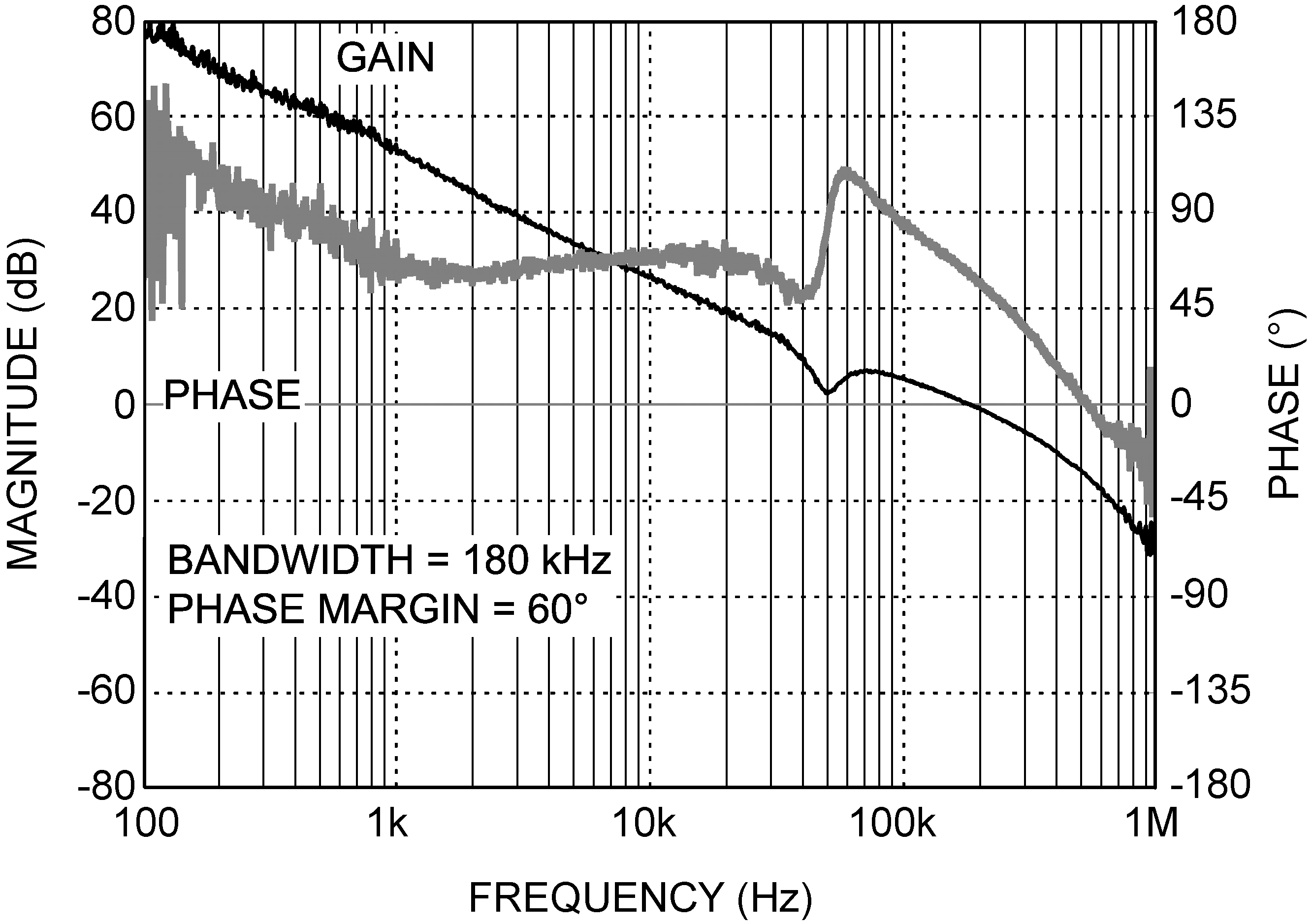
VIN = 12 V VOUT = 3.3 V L = 1.5 µH
COUT = 44 µF IOUT = 1 A
Figure 9. Magnitude vs Frequency
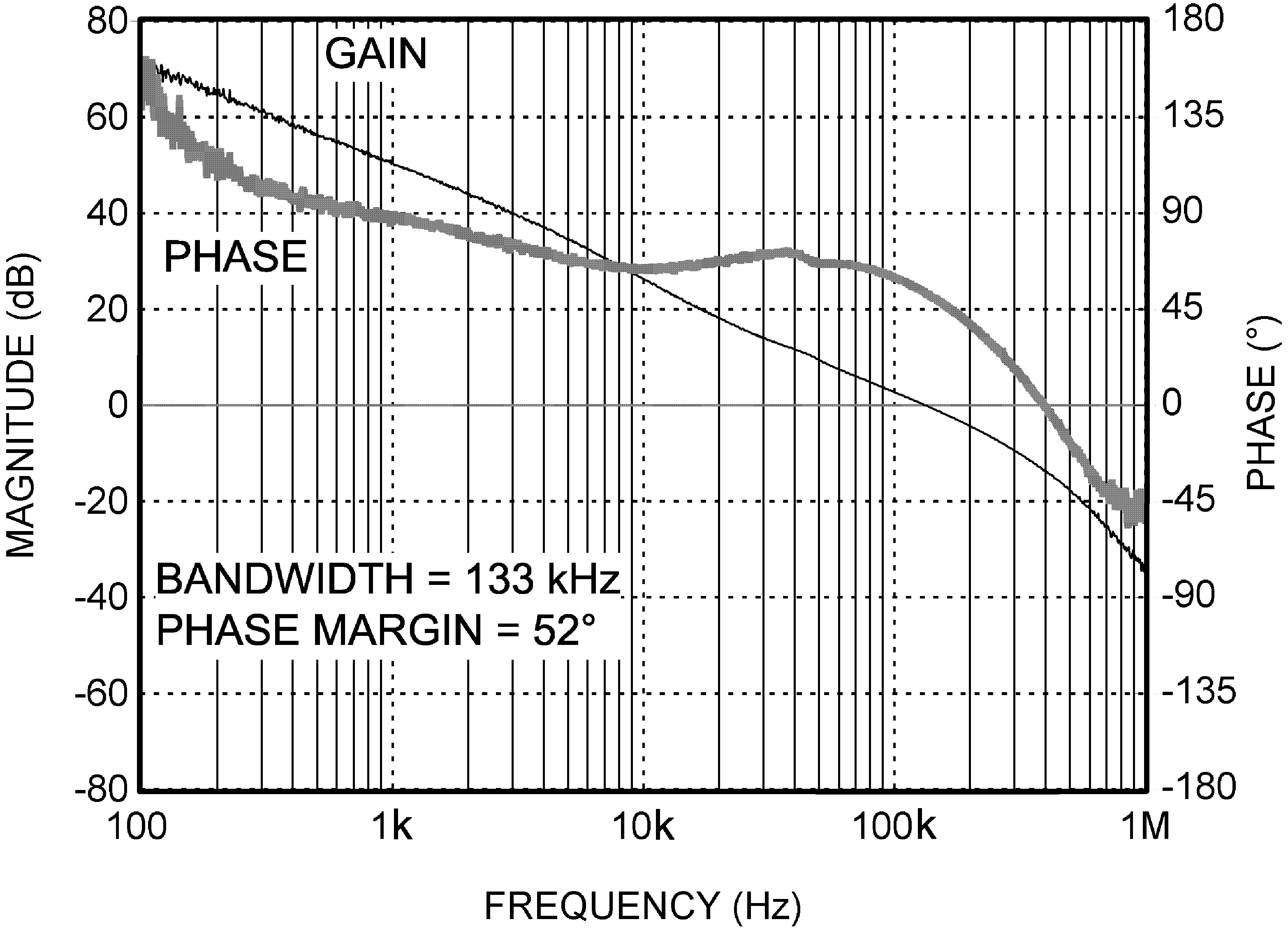
LMR12015 LMR12020 301970b5.png
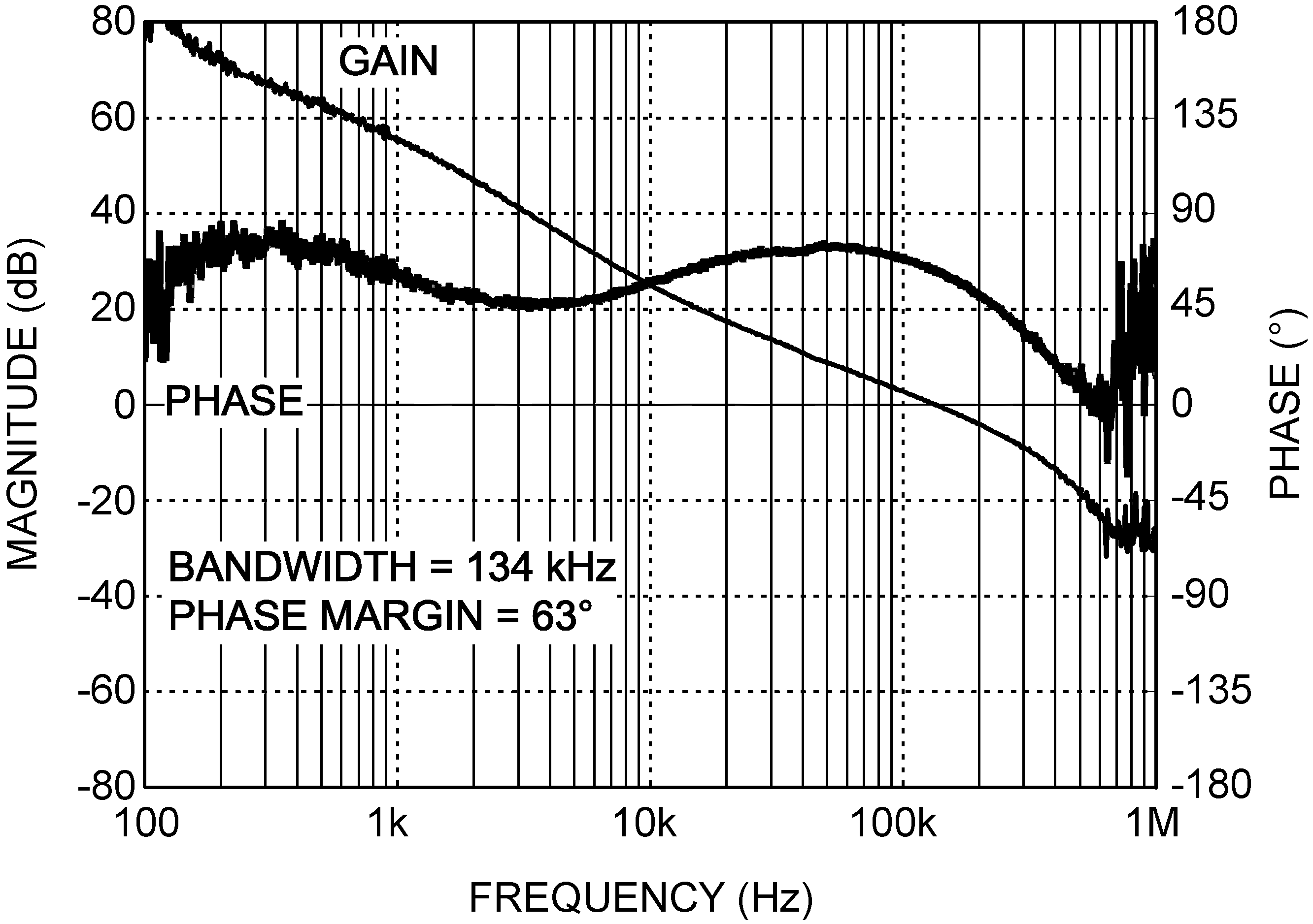
VIN = 5 V VOUT = 1.2 V L = 0.56 µH
COUT = 68 µF IOUT = 1 A
Figure 11. Magnitude vs Frequency
LMR12015 LMR12020 30197056.png
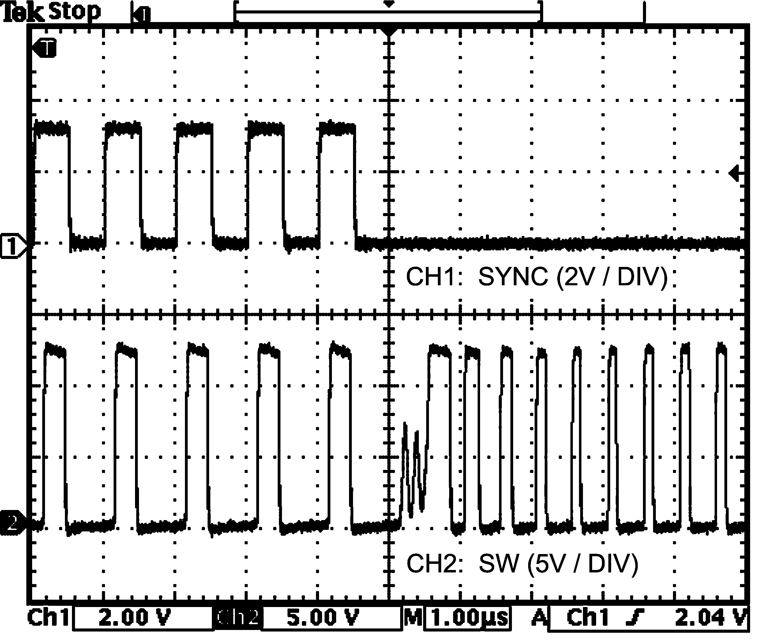
Figure 13. Loss Of Synchronization
LMR12015 LMR12020 30197029.png
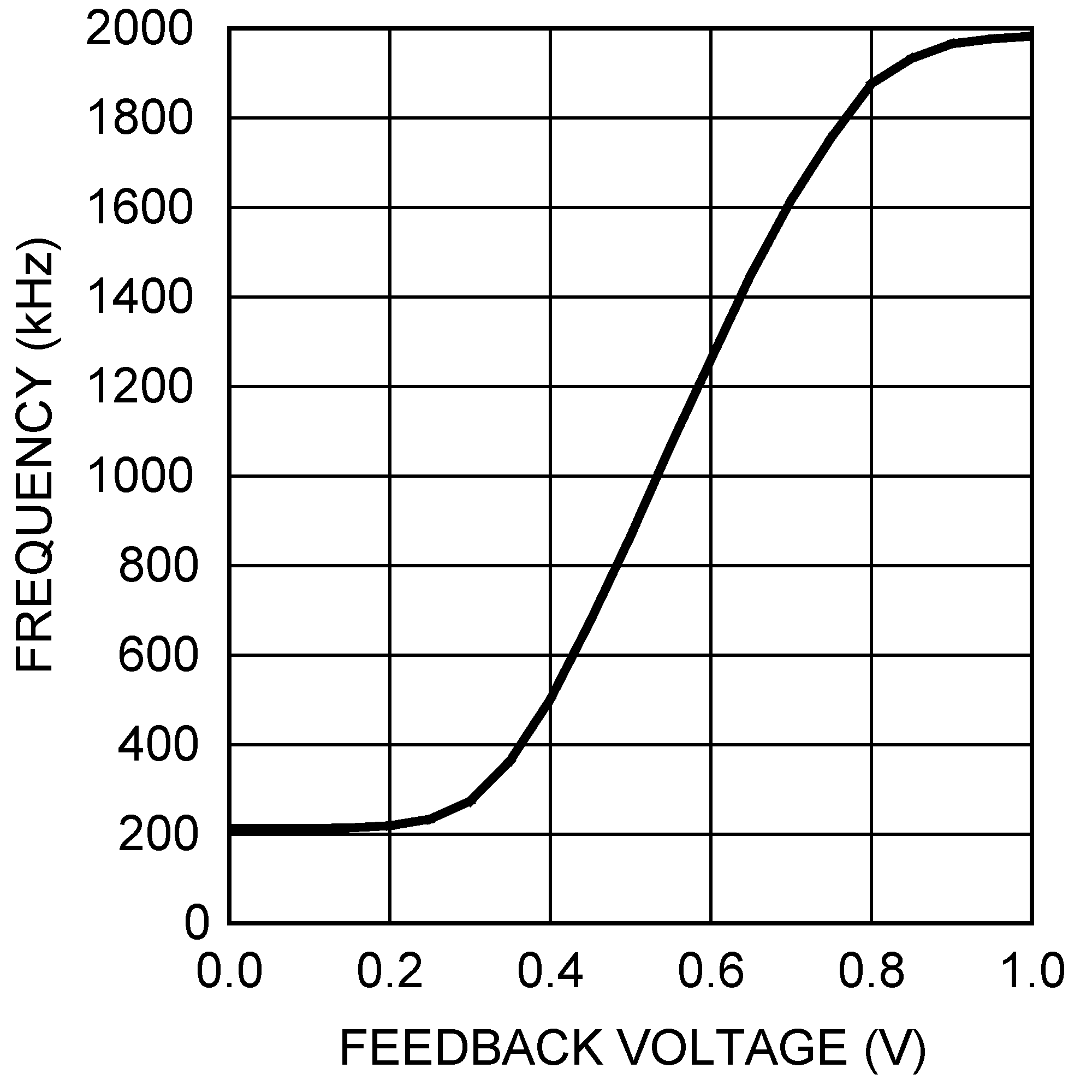
VSYNC = GND
Figure 15. Oscillator Frequency vs VFB
LMR12015 LMR12020 30197031.png
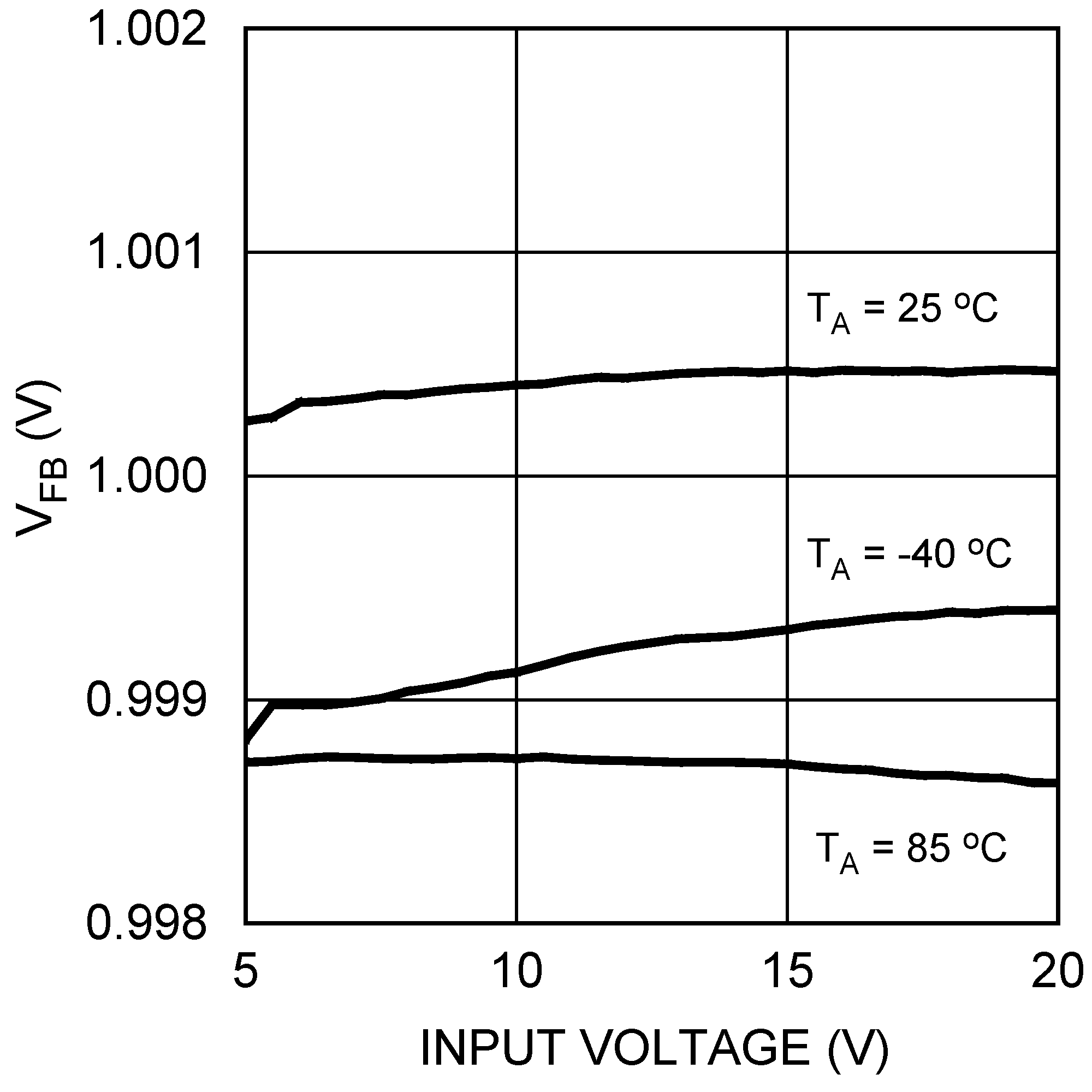
Figure 17. VFB vs VIN
LMR12015 LMR12020 30197033.png
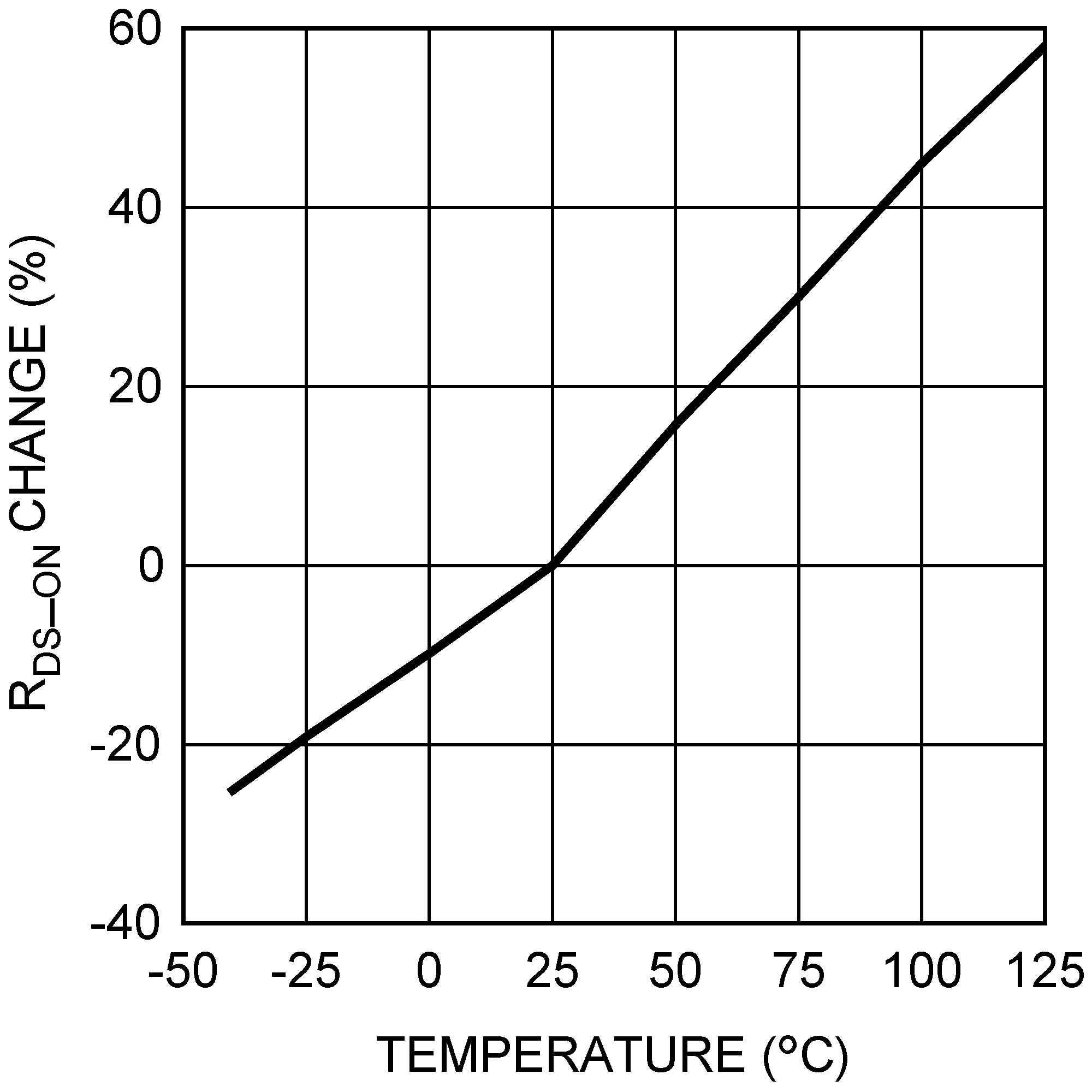
Figure 19. RDSON vs Temperature
LMR12015 LMR12020 30197035.png
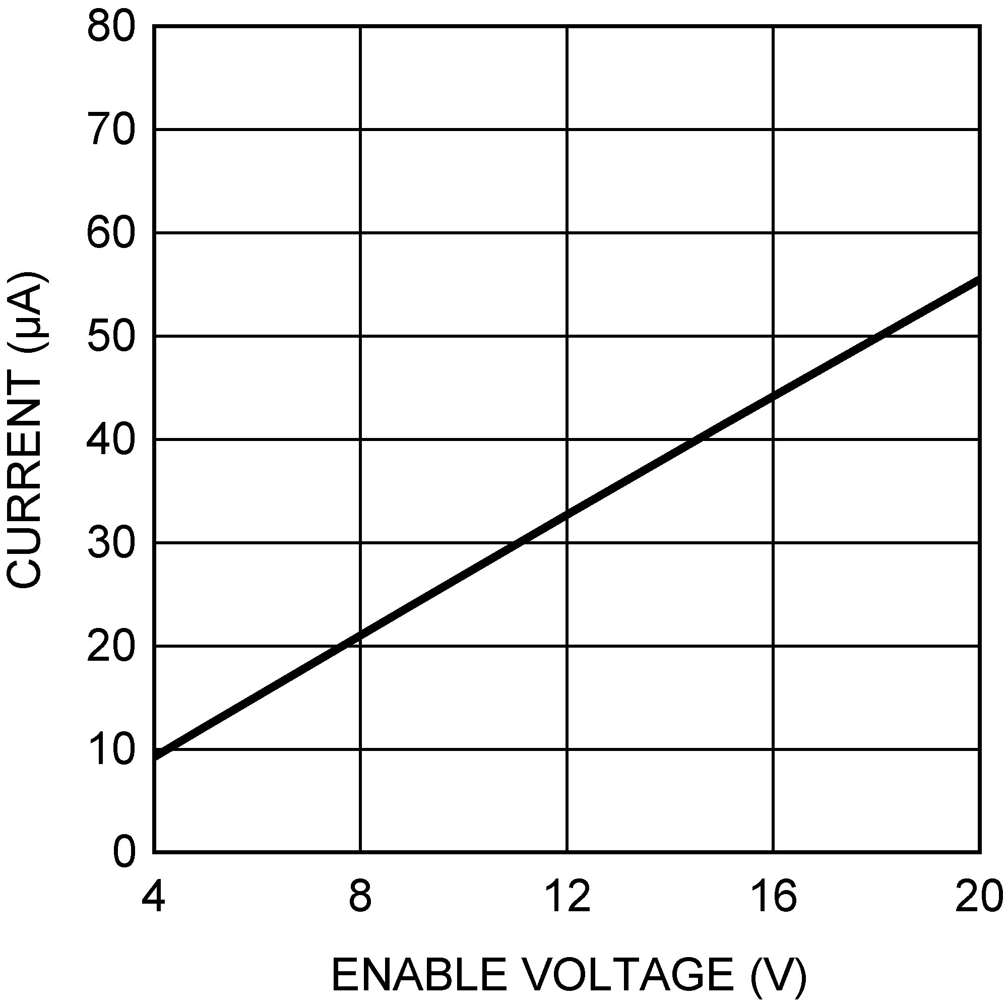
Figure 21. IEN vs VEN
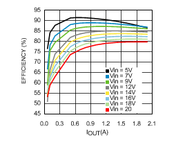
LMR12015 LMR12020 301970b7.gif
VIN = 3.3 V ƒSW = 2 MHz
Refer To Figure 39
Figure 2. Efficiency vs Load Current
LMR12015 LMR12020 301970b0.png
Figure 4. Short Circuit
LMR12015 LMR12020 30197053.png
Figure 6. Soft Start
LMR12015 LMR12020 301970b2.png
VIN = 12 V VOUT = 5 V L = 2.2 µH
COUT = 44 µF IOUT = 1 A
Figure 8. Magnitude vs Frequency
LMR12015 LMR12020 301970b4.png
VIN = 5 V VOUT = 1.8 V L = 1 µH
COUT = 44 µF IOUT = 1 A
Figure 10. Magnitude vs Frequency
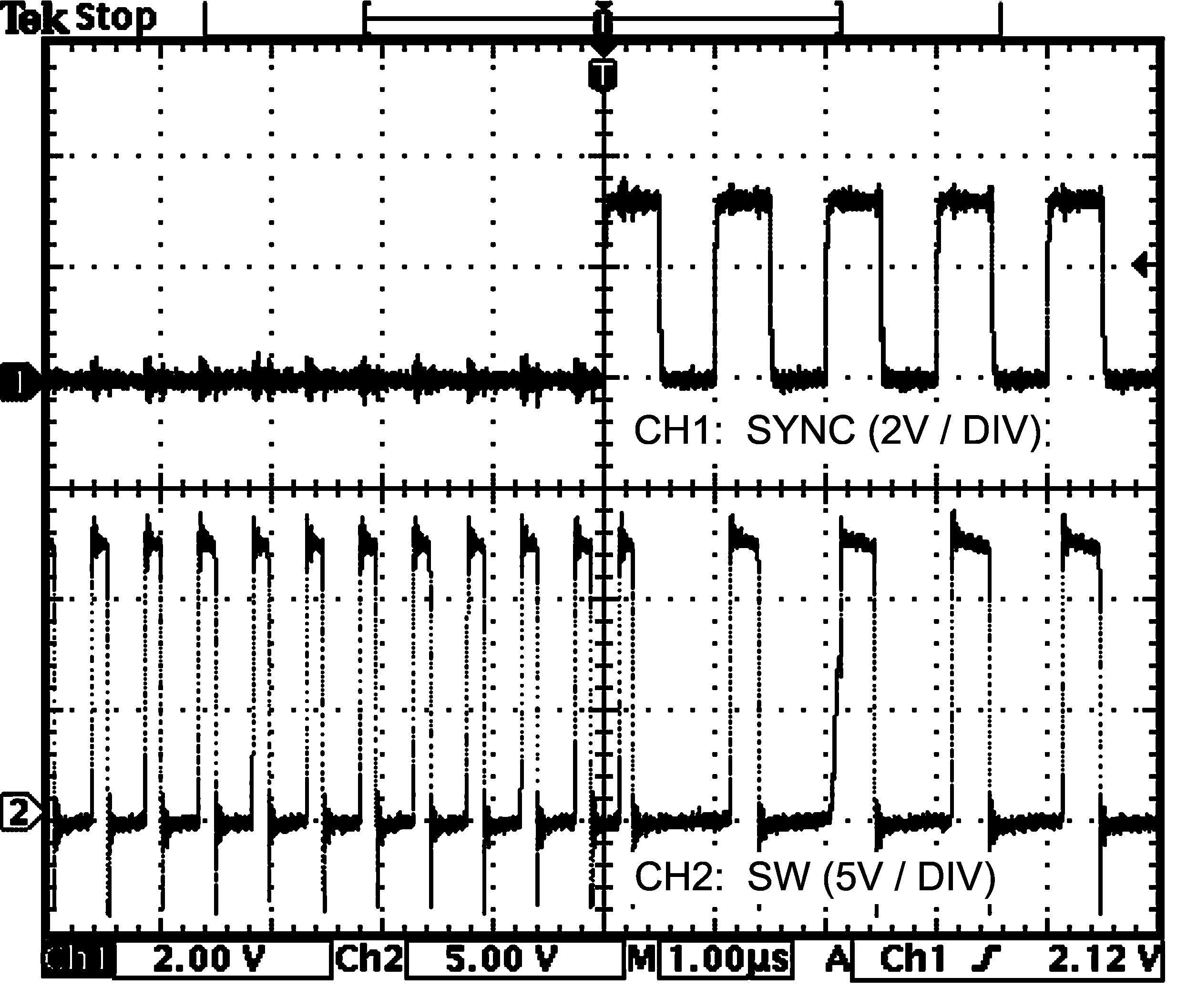
LMR12015 LMR12020 30197055.png
Figure 12. Sync Functionality
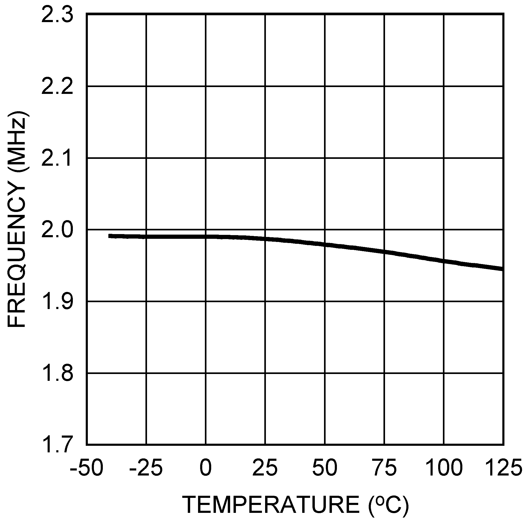
LMR12015 LMR12020 30197028.png
VSYNC = GND
Figure 14. Oscillator Frequency vs Temperature
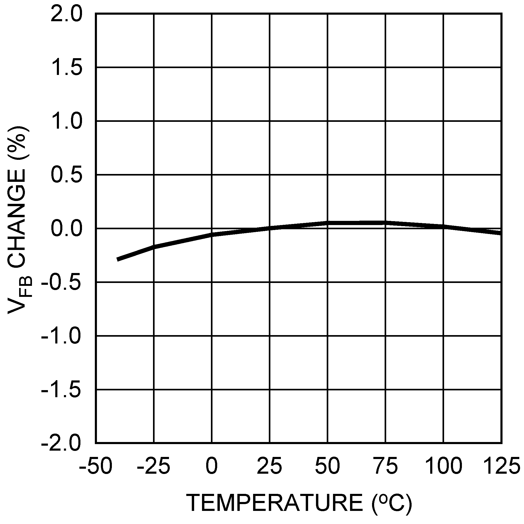
LMR12015 LMR12020 30197030.png
Figure 16. VFB vs Temperature
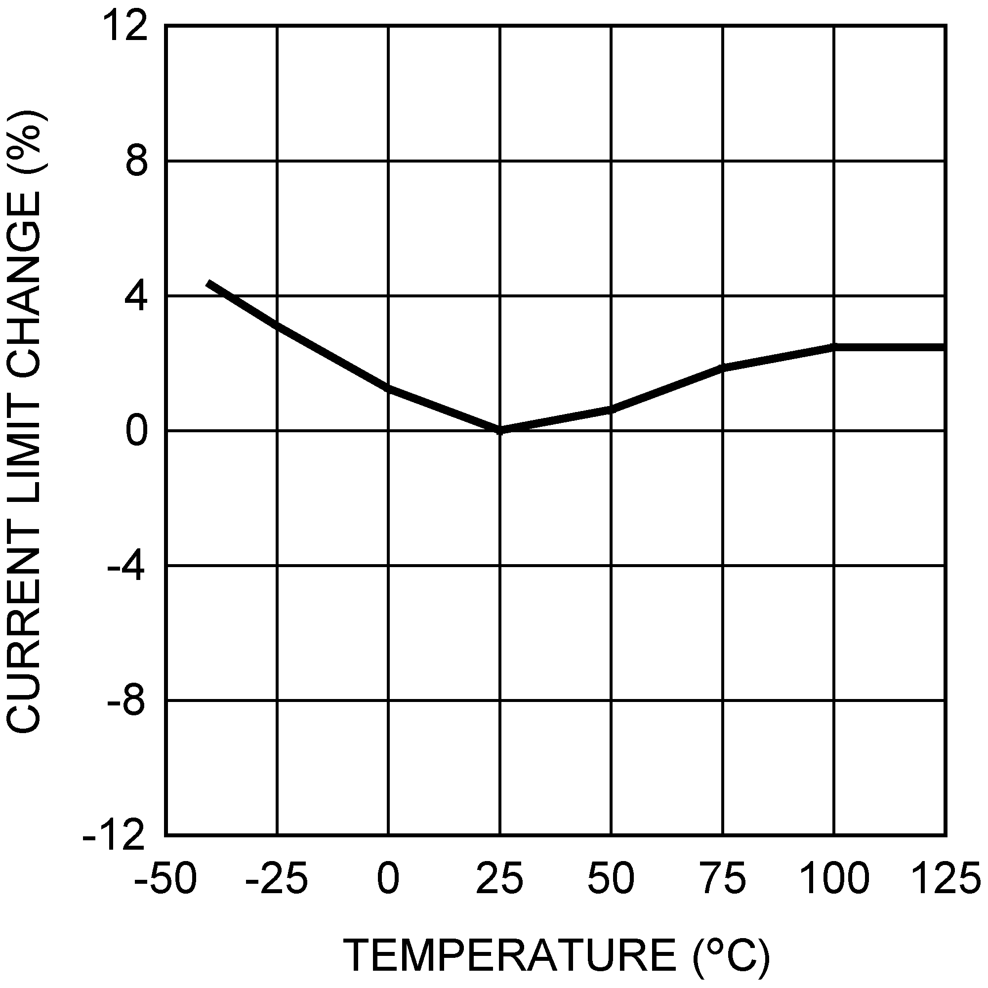
LMR12015 LMR12020 30197032.png
VIN = 12 V
Figure 18. Current Limit vs Temperature
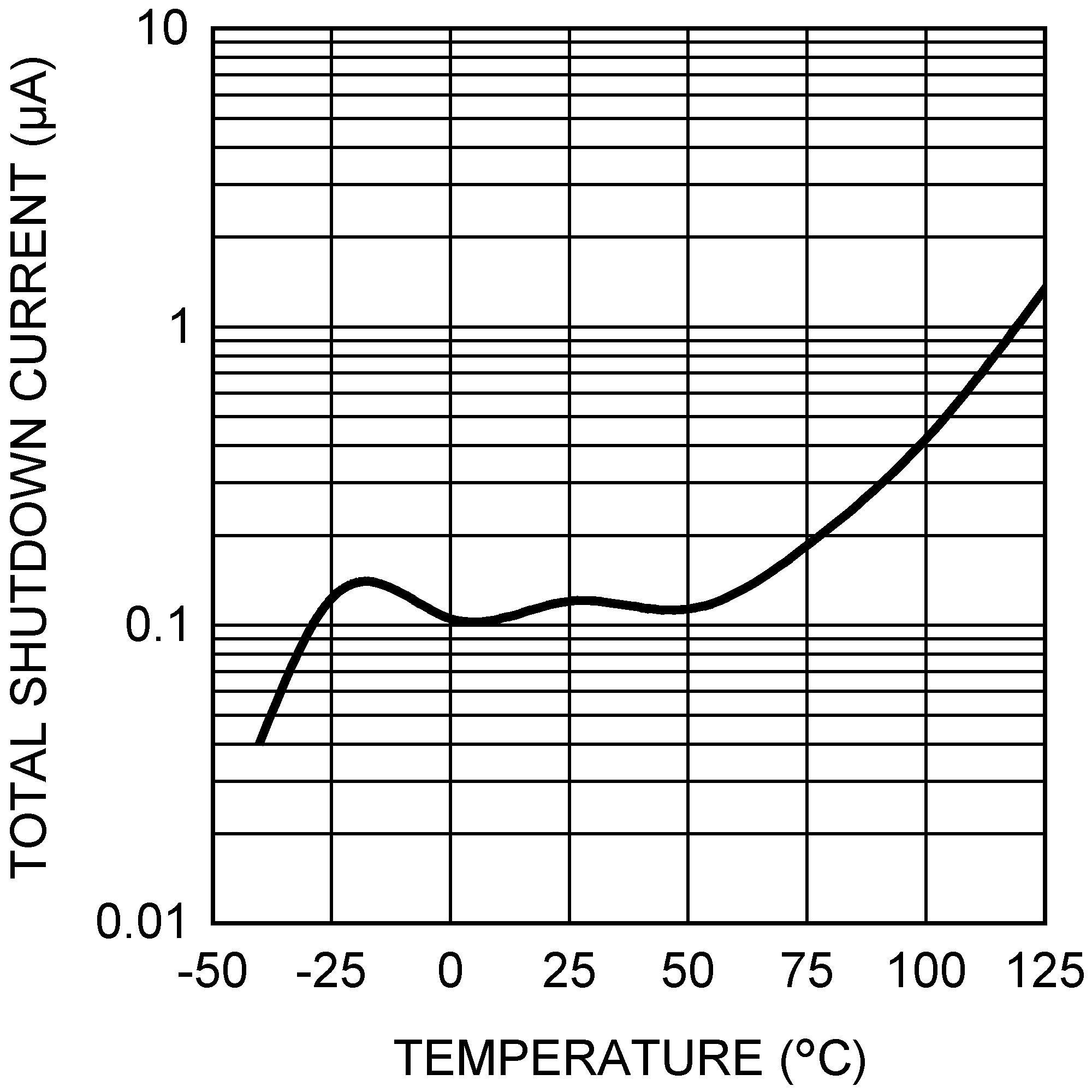
LMR12015 LMR12020 30197034.png
IQ = IAVIN + IPVIN
Figure 20. IQ (Shutdown) vs Temperature