SNVSAH3E February 2018 – July 2020 LMR23625
PRODUCTION DATA
- 1 Features
- 2 Applications
- 3 Description
- 4 Revision History
- 5 Pin Configuration and Functions
- 6 Specifications
-
7 Detailed Description
- 7.1 Overview
- 7.2 Functional Block Diagram
- 7.3
Feature Description
- 7.3.1 Fixed-Frequency Peak-Current-Mode Control
- 7.3.2 Adjustable Output Voltage
- 7.3.3 Enable/Sync
- 7.3.4 VCC, UVLO
- 7.3.5 Minimum ON-time, Minimum OFF-time and Frequency Foldback at Drop-out Conditions
- 7.3.6 Internal Compensation and CFF
- 7.3.7 Bootstrap Voltage (BOOT)
- 7.3.8 Overcurrent and Short-Circuit Protection
- 7.3.9 Thermal Shutdown
- 7.4 Device Functional Modes
-
8 Application and Implementation
- 8.1 Application Information
- 8.2
Typical Applications
- 8.2.1 Design Requirements
- 8.2.2
Detailed Design Procedure
- 8.2.2.1 Custom Design With WEBENCH® Tools
- 8.2.2.2 Output Voltage Setpoint
- 8.2.2.3 Switching Frequency
- 8.2.2.4 Inductor Selection
- 8.2.2.5 Output Capacitor Selection
- 8.2.2.6 Feed-forward Capacitor
- 8.2.2.7 Input Capacitor Selection
- 8.2.2.8 Bootstrap Capacitor Selection
- 8.2.2.9 VCC Capacitor Selection
- 8.2.2.10 Undervoltage Lockout Set-Point
- 8.2.3 Application Curves
- 9 Power Supply Recommendations
- 10Layout
- 11Device and Documentation Support
- 12Mechanical, Packaging, and Orderable Information
Package Options
Refer to the PDF data sheet for device specific package drawings
Mechanical Data (Package|Pins)
- DDA|8
- DRR|12
Thermal pad, mechanical data (Package|Pins)
Orderable Information
7.3.8 Overcurrent and Short-Circuit Protection
The LMR23625 is protected from overcurrent conditions by cycle-by-cycle current limit on both the peak and valley of the inductor current. Hiccup mode is activated if a fault condition persists to prevent over-heating.
High-side MOSFET over-current protection is implemented by the nature of the peak-current-mode control. The HS switch current is sensed when the HS is turned on after a set blanking time. The HS switch current is compared to the output of the error amplifier (EA) minus slope compensation every switching cycle. See Section 7.2 for more details. The peak current of HS switch is limited by a clamped maximum peak-current threshold IHS_LIMIT which is constant. Thus, the peak current limit of the high-side switch is not affected by the slope compensation and remains constant over the full duty cycle range.
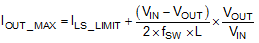
The current going through LS MOSFET is also sensed and monitored. When the LS switch turns on, the inductor current begins to ramp down. The LS switch will not be turned OFF at the end of a switching cycle if its current is above the LS current limit ILS_LIMIT. The LS switch is kept ON so that inductor current keeps ramping down until the inductor current ramps below the LS current limit ILS_LIMIT. Then the LS switch is turned OFF, and the HS switch will be turned on after a dead time. This is somewhat different than the more typical peak current limit and results in Equation 9 for the maximum load current.
If the current of the LS switch is higher than the LS current limit for 64 consecutive cycles, hiccup-current-protection mode is activated. In hiccup mode, the regulator is shut down and kept off for 5 ms typically before the LMR23625 tries to start again. If an overcurrent or short-circuit fault condition still exists, hiccup repeats until the fault condition is removed. Hiccup mode reduces power dissipation under severe overcurrent conditions, prevents over-heating and potential damage to the device.
For FPWM option, the inductor current is allowed to go negative. Should this current exceed IL_NEG, the LS switch is turned off until the next clock cycle. This is used to protect the LS switch from excessive negative current.