SNVSBI9A October 2019 – June 2022 LMR33610
PRODUCTION DATA
- 1 Features
- 2 Applications
- 3 Description
- 4 Revision History
- 5 Device Comparison
- 6 Pin Configuration and Functions
- 7 Specifications
- 8 Detailed Description
-
9 Application and Implementation
- 9.1 Application Information
- 9.2
Typical Application
- 9.2.1 Design Requirements
- 9.2.2
Detailed Design Procedure
- 9.2.2.1 Custom Design With WEBENCH® Tools
- 9.2.2.2 Choosing the Switching Frequency
- 9.2.2.3 Setting the Output Voltage
- 9.2.2.4 Inductor Selection
- 9.2.2.5 Output Capacitor Selection
- 9.2.2.6 Input Capacitor Selection
- 9.2.2.7 CBOOT
- 9.2.2.8 VCC
- 9.2.2.9 CFF Selection
- 9.2.2.10 External UVLO
- 9.2.2.11 Maximum Ambient Temperature
- 9.2.3 Application Curves
- 9.3 What to Do and What Not to Do
- 10Power Supply Recommendations
- 11Layout
- 12Device and Documentation Support
- 13Mechanical, Packaging, and Orderable Information
Package Options
Mechanical Data (Package|Pins)
- DDA|8
Thermal pad, mechanical data (Package|Pins)
- DDA|8
Orderable Information
8.3.3 Current Limit and Short Circuit
The LMR33610 incorporates both peak and valley inductor current limit to provide protection to the device from overloads and short circuits and limit the maximum output current. Valley current limit prevents inductor current runaway during short circuits on the output, while both peak and valley limits work together to limit the maximum output current of the converter. Cycle-by-cycle current limit is used for overloads, while hiccup mode is used for sustained short circuits. Finally, a zero current detector is used on the low-side power MOSFET to implement DEM at light loads (see the Glossary). The typical value of this current limit is found under IZC in the Electrical Characteristics.
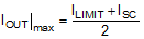
When the device is overloaded, the valley of the inductor current may not reach below ILIMIT (see the Electrical Characteristics) before the next clock cycle. When this occurs, the valley current limit control skips that cycle, causing the switching frequency to drop. Further overload causes the switching frequency to continue to drop, and the inductor ripple current to increase. When the peak of the inductor current reaches the high-side current limit, ISC (see the Electrical Characteristics), the switch duty cycle is reduced and the output voltage falls out of regulation. This represents the maximum output current from the converter and is given approximately by Equation 1.
If, during current limit, the voltage on the FB input falls below about 0.4 V, due to a short circuit, the device enters hiccup mode. In this mode, the device stops switching for tHC (see the System Characteristics), or approximately 94 ms, and then goes through a normal restart with soft start. If the short-circuit condition remains, the device runs in current limit for approximately 20 ms (typical) and then shuts down again. This cycle repeats, as shown in Figure 8-5, as long as the short-circuit-condition persists. This mode of operation reduces the temperature rise of the device during a hard short on the output. The output current is greatly reduced during hiccup mode (see the Typical Characteristics). Once the output short is removed and the hiccup delay is passed, the output voltage recovers normally as shown in Figure 8-6.
 Figure 8-5 Inductor Current Burst in Short-Circuit Mode
 Figure 8-6 Short-Circuit Transient and Recovery