SNVSB53C February   2018  – March 2023 LMZM23600

PRODUCTION DATA  

  1. Features
  2. Applications
  3. Description
  4. Revision History
  5. Device Comparison
  6. Pin Configuration and Functions
  7. Specifications
    1. 7.1 Absolute Maximum Ratings
    2. 7.2 ESD Ratings
    3. 7.3 Recommended Operating Conditions
    4. 7.4 Thermal Information
    5. 7.5 Electrical Characteristics
    6. 7.6 System Characteristics
    7. 7.7 Typical Characteristics
  8. Detailed Description
    1. 8.1 Overview
    2. 8.2 Functional Block Diagram
    3. 8.3 Feature Description
      1. 8.3.1 Control Scheme
      2. 8.3.2 Soft-Start Function
      3. 8.3.3 Enable and External UVLO Function
      4. 8.3.4 Current Limit
      5. 8.3.5 Hiccup Mode
      6. 8.3.6 Power Good (PGOOD) Function
      7. 8.3.7 MODE/SYNC Function
        1. 8.3.7.1 Forced PWM Mode
        2. 8.3.7.2 Auto PFM Mode
        3. 8.3.7.3 Dropout Mode
        4. 8.3.7.4 SYNC Operation
      8. 8.3.8 Thermal Protection
    4. 8.4 Device Functional Modes
      1. 8.4.1 Shutdown
      2. 8.4.2 FPWM Operation
      3. 8.4.3 Auto PFM Mode Operation
  9. Application and Implementation
    1. 9.1 Application Information
    2. 9.2 Typical Applications
      1. 9.2.1 Design Requirements
        1. 9.2.1.1 Maximum Input Voltage for VOUT < 2.5 V
      2. 9.2.2 Detailed Design Procedure
        1. 9.2.2.1 Custom Design With WEBENCH® Tools
        2. 9.2.2.2 Input Capacitor Selection
        3. 9.2.2.3 Output Capacitor Selection
        4. 9.2.2.4 Feedback Voltage Divider for Adjustable Output Voltage Versions
        5. 9.2.2.5 RPU - PGOOD Pullup Resistor
        6. 9.2.2.6 VIN Divider and Enable
      3. 9.2.3 Application Curves
        1. 9.2.3.1 VOUT = 5 V
        2. 9.2.3.2 VOUT = 3.3 V
        3. 9.2.3.3 VOUT = 12 V
        4. 9.2.3.4 VOUT = 15 V
        5. 9.2.3.5 VOUT = 2.5 V
        6. 9.2.3.6 VOUT = 1.2 V and VOUT = 1.8 V
        7. 9.2.3.7 VOUT = 5 V and 3.3 V Fixed Output Options
    3. 9.3 Best Design Practices
    4. 9.4 Power Supply Recommendations
      1. 9.4.1 Supply Voltage Range
      2. 9.4.2 Supply Current Capability
      3. 9.4.3 Supply Input Connections
        1. 9.4.3.1 Voltage Drops
        2. 9.4.3.2 Stability
    5. 9.5 Layout
      1. 9.5.1 Layout Guidelines
        1. 9.5.1.1 Thermal Design
      2. 9.5.2 Layout Examples
  10. 10Device and Documentation Support
    1. 10.1 Device Support
      1. 10.1.1 Third-Party Products Disclaimer
      2. 10.1.2 Development Support
        1. 10.1.2.1 Custom Design With WEBENCH® Tools
    2. 10.2 Documentation Support
      1. 10.2.1 Related Documentation
    3. 10.3 Receiving Notification of Documentation Updates
    4. 10.4 Support Resources
    5. 10.5 Trademarks
    6. 10.6 Electrostatic Discharge Caution
    7. 10.7 Glossary
  11. 11Mechanical, Packaging, and Orderable Information
    1. 11.1 Tape and Reel Information

Package Options

Mechanical Data (Package|Pins)
Thermal pad, mechanical data (Package|Pins)
Orderable Information

Stability

The added inductance of long input cables together with the ceramic (and low ESR) input capacitor can result in an underdamped RLC network at the input of the buck converter. This circuit can cause instability, or overvoltage transients at the VIN pin each time the input supply is cycled on and off. If long wires are used, TI recommends adding some electrolytic bulk capacitance in parallel with the ceramic input capacitor. The ESR of the bulk capacitor improves the damping. Use an electrolytic capacitor with a capacitance at least four times larger than the ceramic input capacitance.

Equation 5. GUID-3FBC9B17-9EB5-4738-857F-8ECE2B926E2A-low.gif

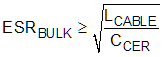
The required ESR from the bulk capacitor depends on the cable inductance.

Equation 6. GUID-C41D2A10-6960-4C12-AF25-941C1B01E3D4-low.gif

For example, two cables (one for VIN and one for GND), each 1 meter (approximately 3 feet) long with approximately 1-mm diameter (18 AWG), placed 1 cm (approximately 0.4 inch) apart forms a rectangular loop resulting in about 1.2 µH of inductance. The inductance in this example can be decreased to almost half if the input wires are twisted. Based on a 10-µF ceramic input capacitor, the recommended parallel CBULK is ≥ 40 µF. Using a 47-µF capacitor is sufficient. Based on about 1.2 µH of inductance and 10 µF of ceramic input capacitance, the recommended ESR of the bulk capacitor is 0.35 Ω or larger. See TI User Guide, Simple Success with Conducted EMI for DC/DC Converters for more details on input filter design.