SNVS083O February 2005 – March 2015 LP2989
PRODUCTION DATA.
- 1 Features
- 2 Applications
- 3 Description
- 4 Revision History
- 5 Pin Configuration and Functions
- 6 Specifications
- 7 Detailed Description
- 8 Application and Implementation
- 9 Power Supply Recommendations
- 10Layout
- 11Device and Documentation Support
- 12Mechanical, Packaging, and Orderable Information
Package Options
Mechanical Data (Package|Pins)
Thermal pad, mechanical data (Package|Pins)
Orderable Information
8 Application and Implementation
NOTE
Information in the following applications sections is not part of the TI component specification, and TI does not warrant its accuracy or completeness. TI’s customers are responsible for determining suitability of components for their purposes. Customers should validate and test their design implementation to confirm system functionality.
8.1 Application Information
The LP2989 is a linear voltage regulator operating from 2.1 V to 16 V on the input and regulates voltages between 2.5 V to 5 V with 0.75% accuracy and 500 mA maximum outputs current. Efficiency is defined by the ratio of output voltage to input voltage because the LP2989 is a linear voltage regulator. To achieve high efficiency, the dropout voltage (VIN – VOUT) must be as small as possible, thus requiring a very low dropout LDO. Successfully implementing an LDO in an application depends on the application requirements. If the requirements are simply input voltage and output voltage, compliance specifications (such as internal power dissipation or stability) must be verified to ensure a solid design. If timing, start-up, noise, PSRR, or any other transient specification is required, the design becomes more challenging. This section discusses the implementation and behavior of the LP2989 LDO.
8.2 Typical Application

8.2.1 Design Requirements
| DESIGN PARAMETER | DESIGN REQUIREMENT |
|---|---|
| Input voltage | 6.5 V, ±10%, |
| Output voltage | 5 V, ±1% |
| Output current | 500 mA (maximum), 1 mA (minimum) |
| RMS noise, 100 Hz to 100 kHz | 18 μVRMS typical |
| PSRR at 1 kHz | 60 dB typical |
8.2.2 Detailed Design Procedure
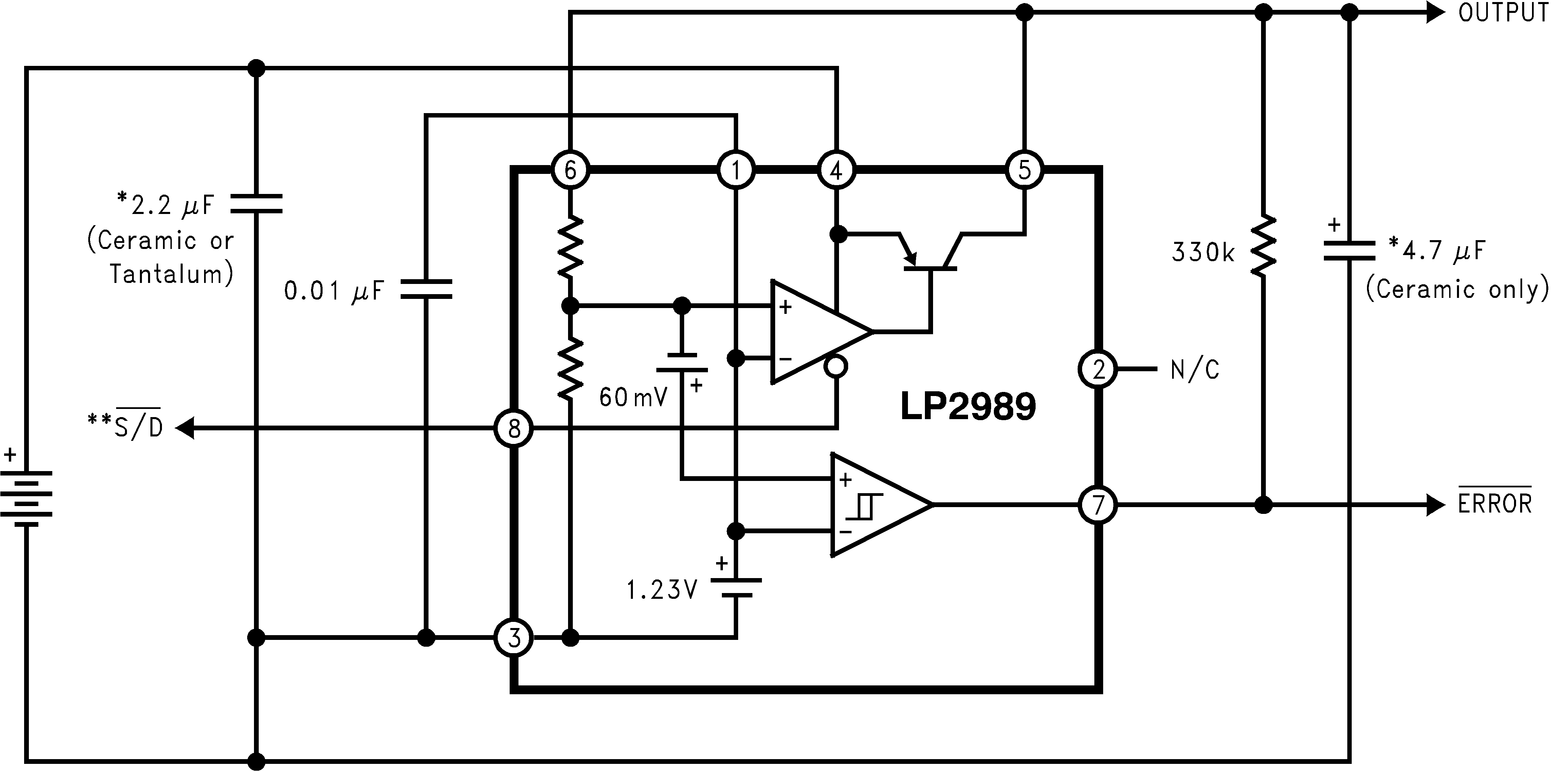
At 500-mA loading, the dropout of the LP2989 has 650-mV maximum dropout over temperature, thus an 1500-mV headroom is sufficient for operation over both input and output voltage accuracy. The efficiency of the LP2989 in this configuration is VOUT / VIN = 76.9%. To achieve the smallest form factor, the WSON package is selected. Input and output capacitors are selected in accordance with the capacitor recommendations. Ceramic capacitances of 2.2 μF for the input and one 4.7-μF capacitor for the output are selected. With an efficiency of 76.9% and a 500-mA maximum load, the internal power dissipation is 750 mW, which corresponds to a 26.1°C junction temperature rise for the WSON package. With an 85°C maximum ambient temperature, the junction temperature is at 111.1°C. To minimize noise, a bypass capacitance (CBYPASS) of 0.01 µF is placed from the BYPASS pin (device pin 1) to device ground (device pin 3).
8.2.2.1 WSON Package Devices
The LP2989 is offered in the 8-lead WSON surface mount package to allow for increased power dissipation compared to the SOIC and VSSOP packages. For details on thermal performance as well as mounting and soldering specifications, refer to Application Note AN-1187 Leadless Leadframe Package (LLP) (SNOA401).
For output voltages < 2 V, see LP2989LV (SNVS086) data sheet.
8.2.2.2 External Capacitors
Like any low-dropout regulator, the LP2989 requires external capacitors for regulator stability. These capacitors must be correctly selected for good performance.
8.2.2.2.1 Input Capacitor
An input capacitor whose value is at least 2.2 µF is required between the LP2989 input and ground (the amount of capacitance may be increased without limit).
Characterization testing performed on the LP2989 has shown that if the value of actual input capacitance drops below about 1.5 µF, an unstable operating condition may result. Therefore, the next larger standard size (2.2 µF) is specified as the minimum required input capacitance. Capacitor tolerance and temperature variation must be considered when selecting a capacitor (see Capacitor Characteristics section) to assure the minimum requirement of 1.5 µF is met over all operating conditions.
The input capacitor must be located at a distance of not more than 0.5 inches from the input pin and returned to a clean analog ground. Any good quality ceramic or tantalum may be used for this capacitor, assuming the minimum capacitance requirement is met.
8.2.2.2.2 Output Capacitor
The LP2989 requires a ceramic output capacitor whose value is at least 4.7 µF. The actual amount of capacitance on the output must never drop below about 3.5 µF or unstable operation may result. For this reason, capacitance tolerance and temperature characteristics must be considered when selecting an output capacitor.
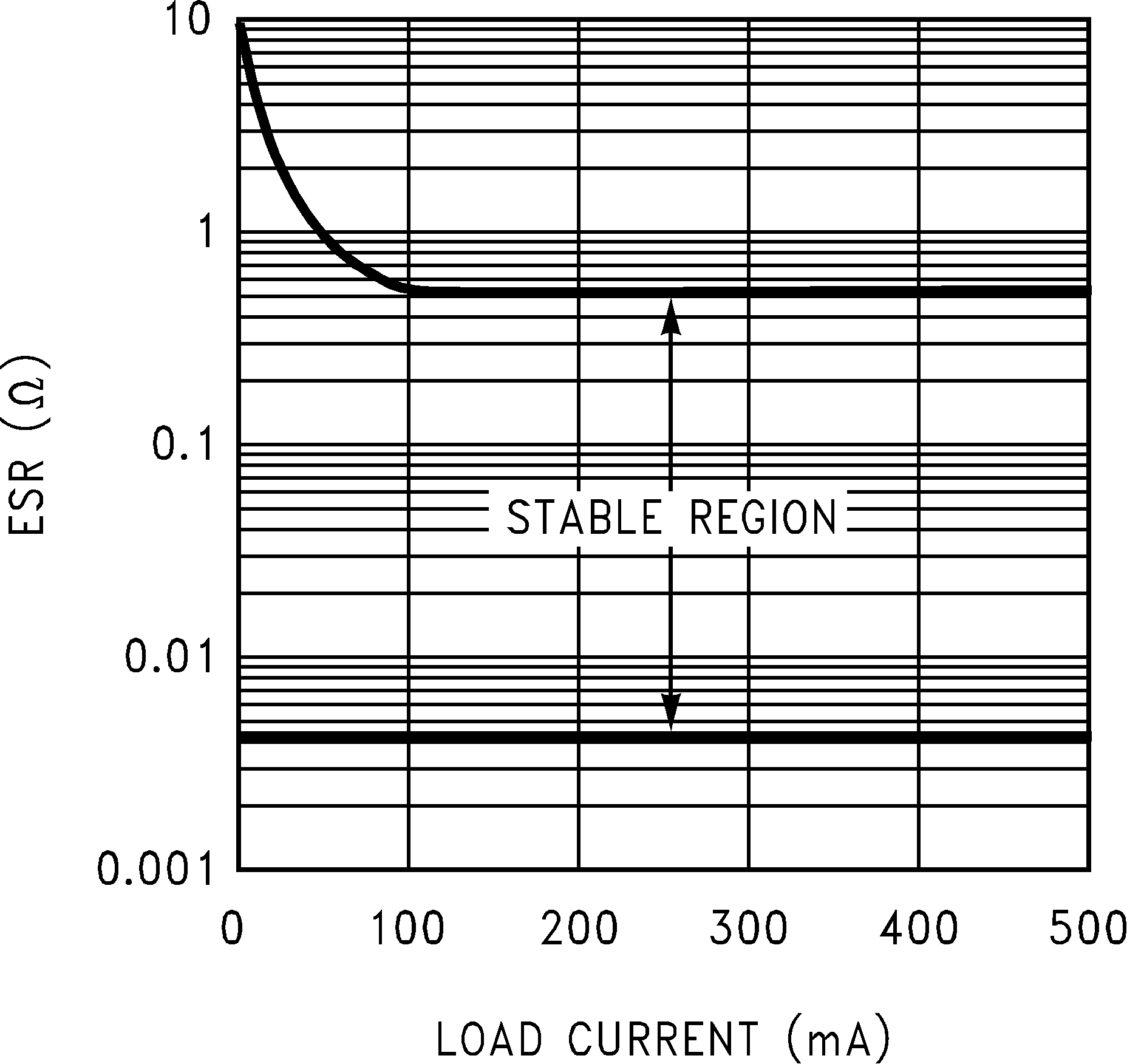
The LP2989 is designed specifically to work with ceramic output capacitors, using circuitry which allows the regulator to be stable across the entire range of output current with an output capacitor whose ESR is as low as 4 mΩ. It may also be possible to use Tantalum or film capacitors at the output, but these are not as attractive for reasons of size and cost (see the Capacitor Characteristics section).
The output capacitor must meet the requirement for minimum amount of capacitance and also have an equivalent series resistance (ESR) value which is within the stable range. Curves are provided which show the stable ESR range as a function of load current (see Figure 41).
 Figure 41. Stable Region for Output Capacitor ESR
NOTE
Important: The output capacitor must maintain its ESR within the stable region over the full operating temperature range of the application to assure stability.
It is important to remember that capacitor tolerance and variation with temperature must be considered when selecting an output capacitor so that the minimum required amount of output capacitance is provided over the full operating temperature range. (See the Capacitor Characteristics section.)
The output capacitor must be located not more than 0.5 inches from the OUT pin and returned to a clean analog ground.
8.2.2.2.3 Noise Bypass Capacitor
Connecting a 10-nF capacitor to the BYPASS pin significantly reduces noise on the regulator output. However, the capacitor is connected directly to a high-impedance circuit in the bandgap reference.
Because this circuit has only a few microamperes flowing in it, any significant loading on this node will cause the regulated output voltage to drop. For this reason, DC leakage current through the noise bypass capacitor must never exceed 100 nA, and should be kept as low as possible for best output voltage accuracy.
The types of capacitors best suited for the noise bypass capacitor are ceramic and film. High-quality ceramic capacitors with either NPO or COG dielectric typically have very low leakage. Ten-nF polypropolene and polycarbonate film capacitors are available in small surface-mount packages and typically have extremely low leakage current.
8.2.2.3 Capacitor Characteristics
8.2.2.3.1 Ceramic
The LP2989 was designed to work with ceramic capacitors on the output to take advantage of the benefits they offer: for capacitance values in the 4.7 µF range, ceramics are the least expensive and also have the lowest ESR values (which makes them best for eliminating high-frequency noise). The ESR of a typical 4.7-µF ceramic capacitor is in the range of 10 mΩ to 15 mΩ, which easily meets the ESR limits required for stability by the LP2989.
One disadvantage of ceramic capacitors is that their capacitance can vary with temperature. Many large-value ceramic capacitors (≥ 2.2 µF) are manufactured with the Z5U or Y5V temperature characteristic, which results in the capacitance dropping by more than 50% as the temperature goes from 25°C to 85°C.
This could cause problems if a 4.7-µF capacitor were used on the output because it will drop down to approximately 2.4 µF at high ambient temperatures (which could cause the LP2989 to oscillate). Another significant problem with Z5U and Y5V dielectric devices is that the capacitance drops severely with applied voltage. A typical Z5U or Y5V capacitor can lose 60% of its rated capacitance with half of the rated voltage applied to it.
For these reasons, X7R and X5R type ceramic capacitors must be used on the input and output of the LP2989.
8.2.2.3.2 Tantalum
Tantalum capacitors are less desirable than ceramics for use as output capacitors because they are typically more expensive when comparing equivalent capacitance and voltage ratings in the 1 µF to 4.7 µF range.
Another important consideration is that Tantalum capacitors have higher ESR values than equivalent size ceramics; while it may be possible to find a Tantalum capacitor with an ESR value within the stable range, it would have to be larger in capacitance (which means bigger and more costly) than a ceramic capacitor with the same ESR value.
It should also be noted that the ESR of a typical Tantalum will increase about 2:1 as the temperature goes from 25°C down to −40°C, so some guard band must be allowed.
Tantalum capacitors may be used on the input as long as the requirement for minimum capacitance is met.
8.2.2.3.3 Film
Polycarbonate and polypropelene film capacitors have excellent electrical performance: their ESR is the lowest of the three types listed, their capacitance is very stable with temperature, and DC leakage current is extremely low.
One disadvantage is that film capacitors are larger in physical size than ceramic or tantalum which makes film a poor choice for either input or output capacitors.
However, their low leakage makes them a good choice for the noise bypass capacitor. Because the required amount of capacitance is only 0.01 µF, small surface-mount film capacitors are available in this size.
8.2.2.4 Reverse Input-Output Voltage
The PNP power transistor used as the pass element in the LP2989 has an inherent diode connected between the regulator output and input.
During normal operation (where the input voltage is higher than the output) this diode is reverse-biased.
However, if the output is pulled above the input, this diode will turn on and current will flow into the regulator output.
In such cases, a parasitic SCR can latch which will allow high current to flow into VIN can damage the part.
In any application where the output may be pulled above the input, an external Schottky diode must be connected from VIN to VOUT (cathode on VIN, anode on VOUT), to limit the reverse voltage across the LP2989 to 0.3 V (see the Absolute Maximum Ratings table).
8.2.3 Application Curves
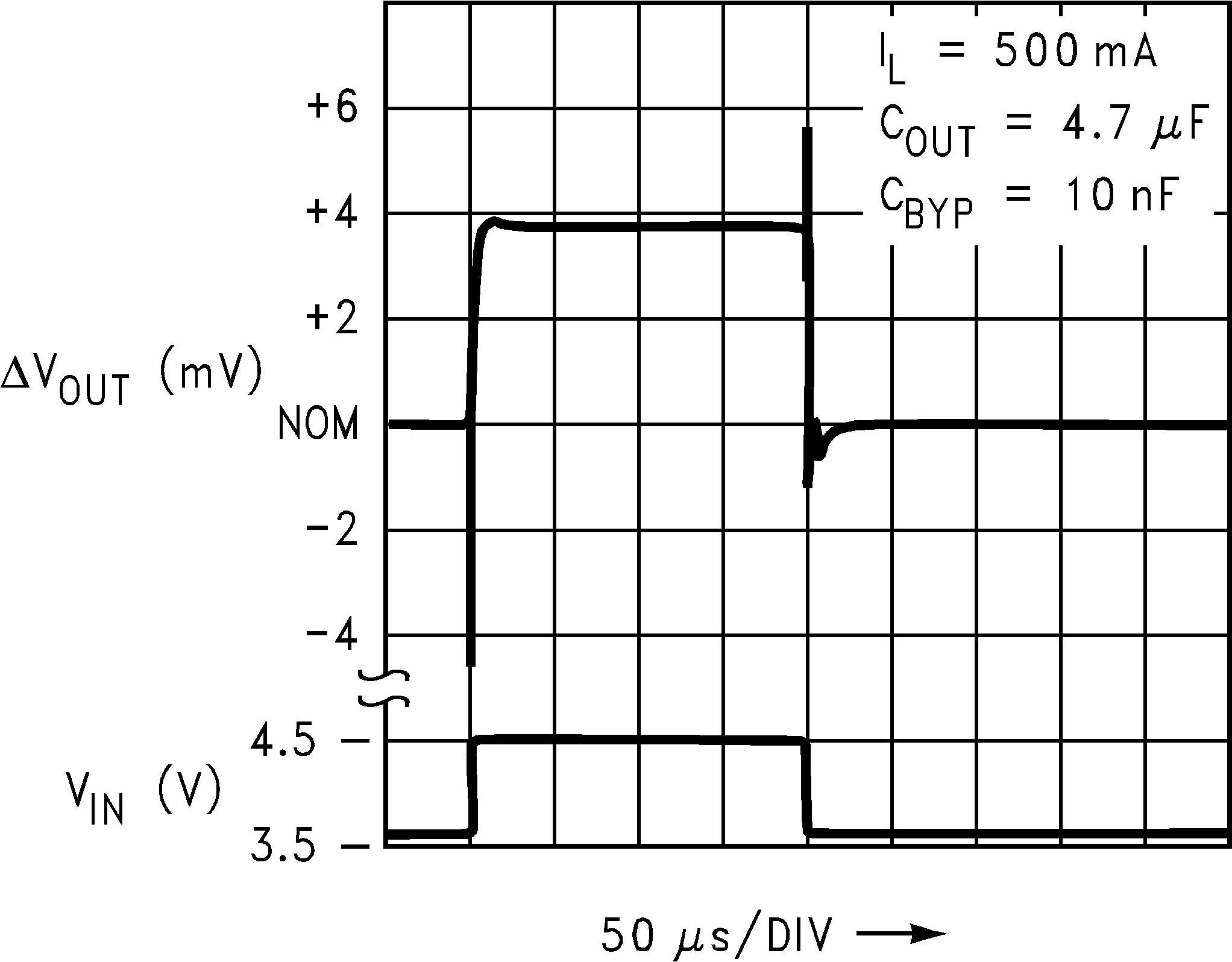
 Figure 42. Line Transient Response
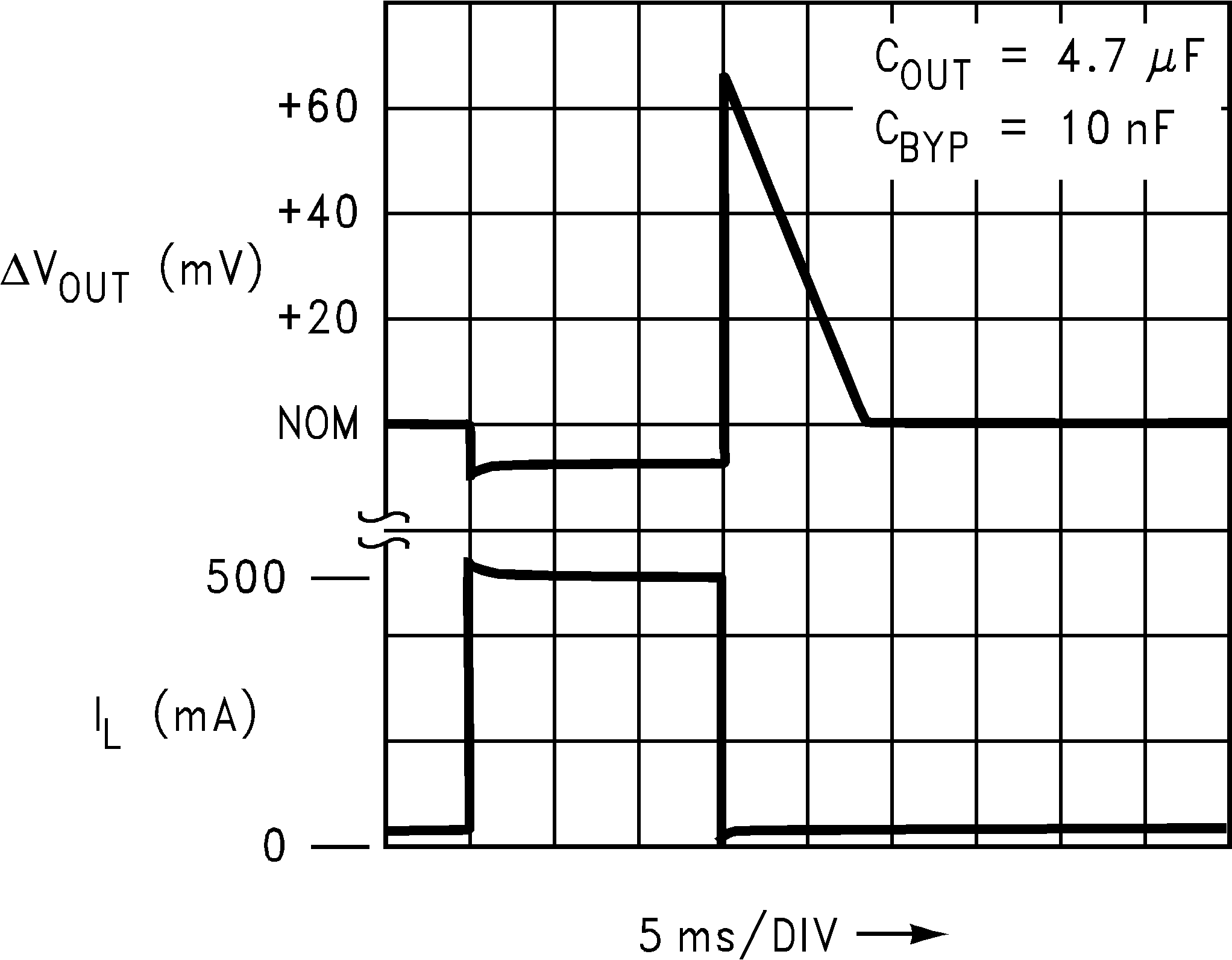
 Figure 43. Load Transient Response