SNVS086K May 2000 – July 2015 LP2989LV
PRODUCTION DATA.
- 1 Features
- 2 Applications
- 3 Description
- 4 Revision History
- 5 Pin Configuration and Functions
- 6 Specifications
- 7 Detailed Description
- 8 Application and Implementation
- 9 Power Supply Recommendations
- 10Layout
- 11Device and Documentation Support
- 12Mechanical, Packaging, and Orderable Information
Package Options
Mechanical Data (Package|Pins)
- D|8
Thermal pad, mechanical data (Package|Pins)
Orderable Information
7 Detailed Description
7.1 Overview
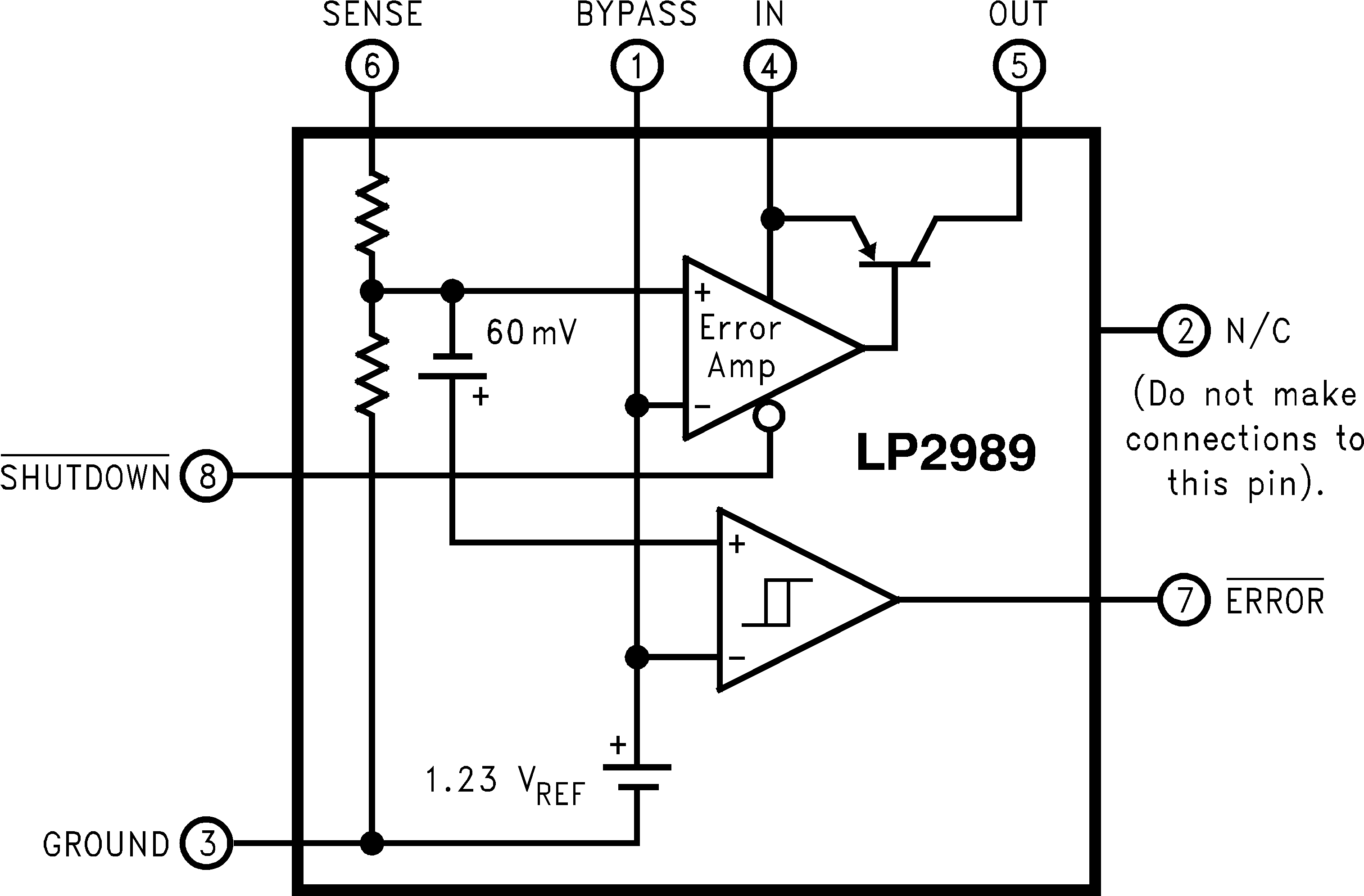
The LP2989LV device is a very high-accuracy micro-power voltage regulator with low quiescent current (75 μA typical) and low dropout voltage (typical 40 mV at light loads and 380 mV at 100 mA). It is ideally suited for use in battery-powered systems. The LP2989LV block diagram contains several features, including:
- Very high-accuracy 1.23-V reference
- SHUTDOWN input
- ERROR flag output
- Internal protection circuitry, such as foldback current limit, and thermal shutdown.
7.2 Functional Block Diagram

7.3 Feature Description
7.3.1 High-Accuracy Output Voltage
With special careful design to minimize all contributions to the output voltage error, the LP2989LV distinguishes itself as a very high output-voltage-accuracy micropower LDO. This includes a tight initial tolerance (0.75% typical, A grade), extremely good line regulation (0.005%/V typical), and a very low output-noise voltage
(10 µVRMS typical), making the device an ideal low-power voltage reference.
7.3.2 Sleep Mode
When pulling SHUTDOWN pin to low levels, the LP2989LV enters shutdown mode, and a very low quiescent current is consumed. This function is designed for applications which needs a shutdown mode to effectively enhance battery life cycle.
7.3.3 Error Detection Comparator Output
The LP2989LV generates a logic low output whenever its output falls out of regulation by more than approximately 5%. Refer to Application and Implementation for more details.
7.3.4 Short Circuit Protection (Current Limit)
The internal current limit circuit is used to protect the LDO against high-load current faults or shorting events. The LDO is not designed to operate in a steady-state current limit. During a current-limit event, the LDO sources constant current. Therefore, the output voltage falls when load impedance decreases. Note also that if a current limit occurs and the resulting output voltage is low, excessive power may be dissipated across the LDO, resulting in a thermal shutdown of the output. A foldback feature limits the short-circuit current to protect the regulator from damage under all load conditions. If OUT is forced below 0 V before EN goes high and the load current required exceeds the foldback current limit, the device may not start correctly.
7.3.5 Thermal Protection
The device contains a thermal shutdown protection circuit to turn off the output current when excessive heat is dissipated in the LDO. The thermal time-constant of the semiconductor die is fairly short, and thus the output cycles on and off at a high rate when thermal shutdown is reached until the power dissipation is reduced. The internal protection circuitry of the device is designed to protect against thermal overload conditions. The circuitry is not intended to replace proper heat sinking. Continuously running the device into thermal shutdown degrades its reliability.
7.4 Device Functional Modes
7.4.1 Operation With 16 V ≥ VIN > VOUT(TARGET) + 1 V
The device operates if the input voltage is equal to, or exceeds VOUT(TARGET) + 1 V. At input voltages below the minimum VIN requirement, the devices does not operate correctly, and output voltage may not reach target value.
7.4.2 Operation with Shutdown Control
If the voltage on the SHUTDOWN pin is less than 0.18 V, the output is ensured to be OFF. When the voltage on the SHUTDOWN pin is more than 1.6 V the output is ensured to be ON. Operating with the SHUTDOWN pin voltage between 0.18 V and 1.6 V is strongly discouraged as the status of the output is not ensured.
7.4.3 Shutdown Input Operation
The LP2989LV is shut off by driving the SHUTDOWN pin low, and turned on by pulling it high. If this feature is not to be used, the SHUTDOWN must be tied to VIN to keep the regulator output on at all times.
To assure proper operation, the signal source used to drive the Shutdown input must be able to swing above and below the specified turn-on/turn-off voltage thresholds listed in Electrical Characteristics under VSD.
To prevent mis-operation, the turnon (and turnoff) voltage signals applied to the SHUTDOWN input must have a slew rate which is ≥ 40 mV/µs.
CAUTION
The regulator output voltage cannot be ensured if a slow-moving AC (or DC) signal is applied that is in the range between the specified turn-on and turn-off voltages listed under the electrical specification VSD (see Electrical Characteristics ).