SNVS086K May 2000 – July 2015 LP2989LV
PRODUCTION DATA.
- 1 Features
- 2 Applications
- 3 Description
- 4 Revision History
- 5 Pin Configuration and Functions
- 6 Specifications
- 7 Detailed Description
- 8 Application and Implementation
- 9 Power Supply Recommendations
- 10Layout
- 11Device and Documentation Support
- 12Mechanical, Packaging, and Orderable Information
Package Options
Mechanical Data (Package|Pins)
- D|8
Thermal pad, mechanical data (Package|Pins)
Orderable Information
10 Layout
10.1 Layout Guidelines
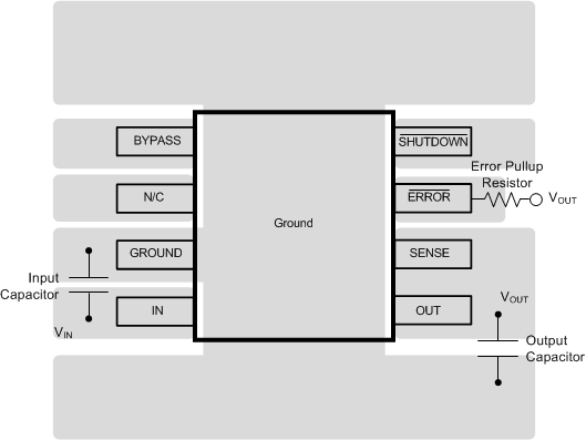
For best overall performance, place all circuit components on the same side of the circuit board and as near as practical to the respective LDO pin connections. Place ground return connections to the input and output capacitor, and to the LDO ground pin as close to each other as possible, connected by a wide, component-side, copper surface. The use of vias and long traces to create LDO circuit connections is strongly discouraged and negatively affects system performance. This grounding and layout scheme minimizes inductive parasitics, and thereby reduces load-current transients, minimizes noise, and increases circuit stability. A ground reference plane is also recommended and is either embedded in the PCB itself or located on the bottom side of the PCB opposite the components. This reference plane serves to assure accuracy of the output voltage, shield noise, and behaves similarly to a thermal plane to spread (or sink) heat from the LDO device. In most applications, this ground plane is necessary to meet thermal requirements.
10.2 Layout Example
 Figure 16. LP2989LV Layout Example
10.2.1 Thermal Considerations
CAUTION
Due to the limited power dissipation characteristics of the available SOIC (D) and WSON (NGN) packages, all possible combinations of output current (IOUT), input voltage (VIN), and ambient temperatures (TA) cannot be ensured.
Power dissipation, PD is calculated from the following formula:
The LP2989LV regulator has internal thermal limiting designed to protect the device during overload conditions. For continuous normal conditions, the recommended maximum operating junction temperature is 125°C. It is important to give careful consideration to all sources of thermal resistance from junction to ambient. Additional heat sources mounted nearby must also be considered.
For surface-mount devices, heat sinking is accomplished by using the heat-spreading capabilities of the PC board and its copper traces. Copper board stiffeners and plated through-holes can also be used to spread the heat generated by power devices.
Example: Given an output voltage of 1.8 V, an input voltage range of 4 V to 6 V, a maximum output current of 100 mA, and a maximum ambient temperature of 50°C, what is the maximum operating junction temperature? The maximum power dissipated by the device (PD(MAX)) is found using the formula in Equation 2:
Using Equation 2, the result is:
where
- IOUT(MAX) = 100 mA
- VIN(MAX) = 6 V
- VOUT = 1.8 V
Using the 8-pin SOIC (D) package, the LP2989LV junction-to-ambient thermal resistance (RθJA) has a rating of 114.5°C/W using the standard JEDEC JESD51-7 PCB (High-K) circuit board.
Thus, The junction temperature rise above ambient (TRISE) using the formula in Equation 3 is:
The junction temperature rise can then be added to the maximum ambient temperature to find the estimated operating junction temperature (TJ) using the formula in Equation 4:
which gives the following results: