SNVS336F June 2006 – August 2015 LP38856
PRODUCTION DATA.
- 1 Features
- 2 Applications
- 3 Description
- 4 Revision History
- 5 Pin Configuration and Functions
- 6 Specifications
- 7 Detailed Description
- 8 Application and Implementation
- 9 Power Supply Recommendations
- 10Layout
- 11Device and Documentation Support
- 12Mechanical, Packaging, and Orderable Information
Package Options
Mechanical Data (Package|Pins)
Thermal pad, mechanical data (Package|Pins)
- KTT|5
Orderable Information
7 Detailed Description
7.1 Overview
The LP38556 is a fast-response, high-current, low-dropout regulator, available in output voltages 0.8 V and 1.2 V. This device is capable of delivering 3-A continuous load current. Standard regulator features, such as overcurrent and overtemperature protection, are also included.
The LP38556 contains several features:
- Low dropout voltage, typical 240 mV at 3-A load.
- Low GND pin current, typical 10 mA at 3-A load.
- A shutdown feature is available, allowing the regulator to consume only 1 µA when EN pin is low.
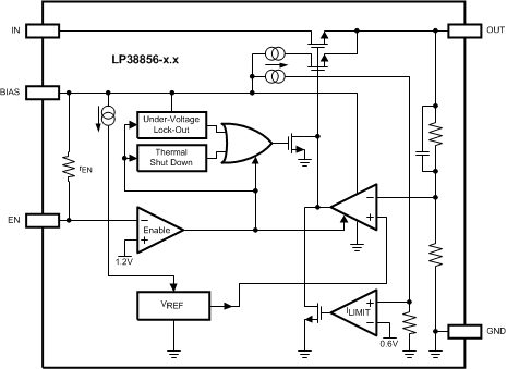
7.2 Functional Block Diagram

7.3 Feature Description
7.3.1 Enable Operation
The enable pin (EN) provides a mechanism to enable, or disable, the regulator output stage. The EN pin has an internal pullup, through a typical 180-kΩ resistor, to VBIAS.
If the EN pin is actively driven, pulling the EN pin above the VEN threshold of 1.25 V (typical) will turn the regulator output on, while pulling the EN pin below the VEN threshold will turn the regulator output off. There is approximately 100 mV of hysteresis built into the enable threshold provide noise immunity.
If the enable function is not needed, the EN pin must be left open, or connected directly to VBIAS. If the EN pin is left open, stray capacitance on this pin must be minimized, otherwise the output turnon will be delayed while the stray capacitance is charged through the internal resistance (rEN).
7.3.2 Input Voltage
The input voltage (VIN) is the high current external voltage rail that will be regulated down to a lower voltage, which is applied to the load. The input voltage must be at least VOUT + VDO, and no higher than whatever value is used for VBIAS.
7.3.3 Bias Voltage
The bias voltage (VBIAS) is a low current external voltage rail required to bias the control circuitry and provide gate drive for the N-FET pass transistor. The bias voltage must be in the range of 3 V to 5.5 V to ensure proper operation of the device.
7.3.4 Undervoltage Lockout
The bias voltage is monitored by a circuit which prevents the device from functioning when the bias voltage is below the undervoltage lock-out (UVLO) threshold of approximately 2.45 V.
As the bias voltage rises above the UVLO threshold the device control circuitry become active. There is approximately 150 mV of hysteresis built into the UVLO threshold to provide noise immunity.
When the bias voltage is between the UVLO threshold and the minimum operating rating value of 3 V the device will be functional, but the operating parameters will not be within the specified limits.
7.3.5 Supply Sequencing
There is no requirement for the order that VIN or VBIAS are applied or removed. However, the output voltage cannot be specified until both VIN and VBIAS are within the range of specified operating values.
If used in a dual-supply system where the regulator load is returned to a negative supply, the output pin must be diode clamped to ground. A Schottky diode is recommend for this diode clamp.
7.3.6 Reverse Voltage
A reverse voltage condition will exist when the voltage at the OUT pin is higher than the voltage at the input pin. Typically this will happen when VIN is abruptly taken low and COUT continues to hold a sufficient charge such that the input to output voltage becomes reversed.
The NMOS pass element, by design, contains no body diode. This means that, as long as the gate of the pass element is not driven, there will not be any reverse current flow through the pass element during a reverse voltage event. The gate of the pass element is not driven when VBIAS is below the UVLO threshold.
When VBIAS is above the UVLO threshold the control circuitry is active and will attempt to regulate the output voltage. Because the input voltage is less than the output voltage, the control circuit will drive the gate of the pass element to the full VBIAS potential when the output voltage begins to fall. In this condition, reverse current will flow from the OUT pin to the IN pin, limited only by the RDS(ON) of the pass element and the output-to-input voltage differential. This condition is outside the specified operating range and must be avoided.
7.4 Device Functional Modes
7.4.1 Operation with 3 V ≤ VBIAS ≤ 5.5 V , VOUT(TARGET) + 0.3 V ≤ VIN ≤ VBIAS
The device operates if the bias voltage is equal to, or exceeds, 3 V; input voltage is equal to, or exceeds, VOUT(TARGET) + 0.3 V. At bias voltages below the minimum VBIAS requirement, the device does not operate correctly, and output voltage may not reach target value.
7.4.2 Operation with VEN Control
If the voltage on the EN pin is less than 1 V, the device is disabled. Raising VEN above 1.5 V initiates the start-up sequence of the device.