SNVS192C October 2002 – November 2015 LP3992
PRODUCTION DATA.
- 1 Features
- 2 Applications
- 3 Description
- 4 Revision History
- 5 Pin Configuration and Functions
- 6 Specifications
- 7 Parameter Measurement Information
- 8 Detailed Description
- 9 Application And Implementation
- 10Power Supply Recommendations
- 11Layout
- 12Device and Documentation Support
- 13Mechanical, Packaging, and Orderable Information
Package Options
Mechanical Data (Package|Pins)
- DBV|5
Thermal pad, mechanical data (Package|Pins)
Orderable Information
8 Detailed Description
8.1 Overview
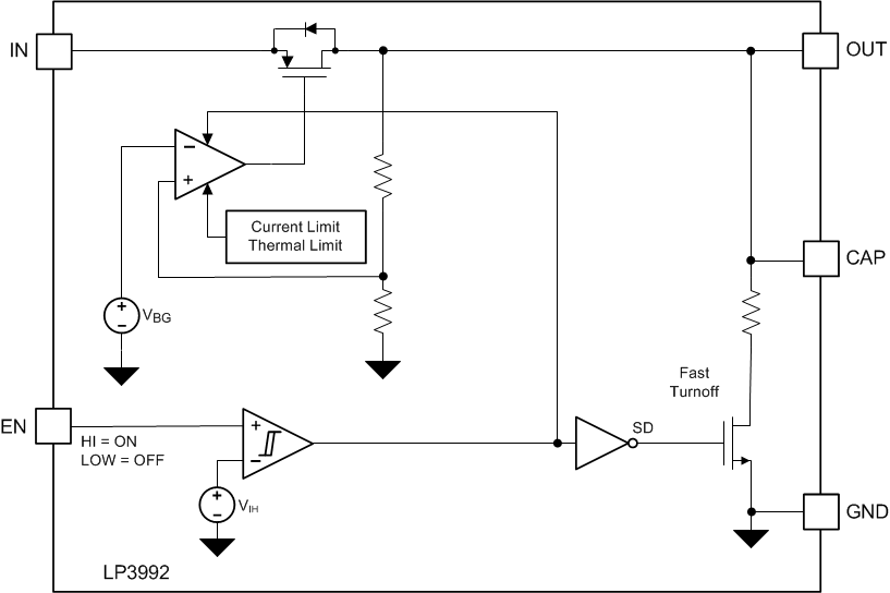
The LP3992 device is a CMOS voltage regulator with a low-input operating-voltage tolerance. Key protection circuits, including thermal-overload and short-circuit protection, are integrated in the device. Using the EN pin, the device may be controlled to provide a SHUTDOWN state, in which negligible supply current is drawn. The LP3992 is designed to be stable with space-saving ceramic capacitors.
8.2 Functional Block Diagram

8.3 Feature Description
8.3.1 Shutdown and Enable
The LP3992 may be switched ON or OFF by a logic input at the EN pin. A high voltage at the EN pin turns the device on. A low voltage on the EN pin will disable the regulator, and will activate the fast turnoff circuitry to discharge the output capacitance. When the regulator is disabled the device typically consumes 3 nA.
If the application does not require the EN feature, the EN pin must be tied to VIN to keep the regulator output permanently on.
To ensure proper operation, the signal source used to drive the EN input must be able to swing above and below the specified turnon or turnoff voltage thresholds listed in the Electrical Characteristics under VIL and VIH.
8.3.2 Fast Turnon and Turnoff
The controlled shutdown feature of the device provides a fast turn off by discharging the output capacitor via an internal FET device. This discharge is current limited by the RDSON of this switch. Fast turnon is ensured by control circuitry within the reference block allowing a very fast ramp of the output voltage to reach the target voltage.
8.4 Device Functional Modes
8.4.1 Enable Operation
The LP3992 may be switched ON or OFF by a logic input at the EN pin. A high voltage at the EN pin turns the device on. A low voltage on the EN pin will disable the regulator, and will activate the fast turnoff circuitry to discharge the output capacitance. When the regulator is disabled the device typically consumes 3 nA.
If the application does not require the EN feature, the EN pin should be tied to VIN to keep the regulator output permanently on.
To ensure proper operation, the signal source used to drive the EN input must be able to swing above and below the specified turnon or turnoff voltage thresholds listed in the Electrical Characteristics under VIL and VIH.