SNVS179F February 2003 – September 2015 LP3995
PRODUCTION DATA.
- 1 Features
- 2 Applications
- 3 Description
- 4 Revision History
- 5 Pin Configuration and Functions
- 6 Specifications
- 7 Parameter Measurement Information
- 8 Detailed Description
- 9 Application and Implementation
- 10Power Supply Recommendations
- 11Layout
- 12Device and Documentation Support
- 13Mechanical, Packaging, and Orderable Information
Package Options
Mechanical Data (Package|Pins)
Thermal pad, mechanical data (Package|Pins)
Orderable Information
8 Detailed Description
8.1 Overview
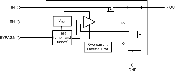
The LP3995 device is a CMOS voltage regulator with a low input operating voltage tolerance. Key protection circuits, including thermal-overload and short-circuit protection, are integrated in the device. Using the EN pin, the device may be controlled to provide a shutdown state, in which negligible supply current is drawn. The LP3995 is designed to be stable with space-saving ceramic capacitors.
8.2 Functional Block Diagram

8.3 Feature Description
8.3.1 Enable (EN)
The EN pin is used to control the ON or OFF status of the LP3995. The EN pin voltage must be higher than the VIH threshold to ensure that the device is fully enabled under all operating conditions.
8.3.2 Fast Turnoff
When the EN pin voltage is lower than the VIL threshold, the output is disabled, and the pull-down circuitry is activated to discharge the output capacitance.
8.3.3 Low Output Noise
The BYPASS pin is an external connection into the LP3995 band-gap circuitry allows the addition of an external capacitor to reduce output noise . A fast-charge circuit is controlled by the enable circuitry to reduce start-up delays. The capacitor on the BYPASS pin also prevents overshoot on the output during startup.
8.3.4 Output Capacitor
The LP3995 requires at least a 1-µF low ESR ceramic capacitor at the OUT pin.
8.3.5 Thermal Overload Protection (TSD)
Thermal shutdown disables the output when the junction temperature rises to approximately 160°C which allows the device to cool. When the junction temperature cools to approximately 140°C, the output circuitry automatically enables. Based on power dissipation, thermal resistance, and ambient temperature, the thermal protection circuit may cycle on and off. This thermal cycling limits the dissipation of the regulator and protects it from damage as a result of overheating. The thermal shutdown circuitry of the LP3995 has been designed to protect against temporary thermal overload conditions. The thermal shutdown circuitry is not intended to replace proper heat-sinking. Continuously running the LP3995 device into thermal shutdown may degrade device reliability.
8.4 Device Functional Modes
8.4.1 Enable Operation
The LP3995 may be switched ON or OFF by a logic input at the EN pin, VEN. A high voltage at this pin turns the device on. When the EN pin is low, the regulator output is off and the device typically consumes 3 nA. If the application does not require the shutdown feature, the EN pin should be tied to VIN to keep the regulator output permanently on. To ensure proper operation, the signal source used to drive the EN input must be able to swing above and below the specified turn-on/off voltage thresholds listed in Electrical Characteristics under VIL and VIH.