SNVS440B May 2007 – March 2016 LP5520
PRODUCTION DATA.
- 1 Features
- 2 Applications
- 3 Description
- 4 Revision History
- 5 Pin Configuration and Function
-
6 Specifications
- 6.1 Absolute Maximum Ratings
- 6.2 ESD Ratings
- 6.3 Recommended Operating Conditions
- 6.4 Thermal Information
- 6.5 Electrical Characteristics
- 6.6 RGB Driver Electrical Characteristics (ROUT, GOUT, BOUT Outputs)
- 6.7 Logic Interface Characteristics
- 6.8 Magnetic Boost DC-DC Converter Electrical Characteristics
- 6.9 I2C Timing Parameters
- 6.10 SPI Timing Requirements
- 6.11 Typical Characteristics
- 7 Detailed Description
- 8 Application and Implementation
- 9 Power Supply Recommendations
- 10Layout
- 11Device and Documentation Support
- 12Mechanical, Packaging, and Orderable Information
Package Options
Mechanical Data (Package|Pins)
- YZR|25
Thermal pad, mechanical data (Package|Pins)
Orderable Information
8 Application and Implementation
NOTE
Information in the following applications sections is not part of the TI component specification, and TI does not warrant its accuracy or completeness. TI’s customers are responsible for determining suitability of components for their purposes. Customers should validate and test their design implementation to confirm system functionality.
8.1 Application Information
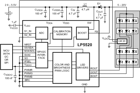
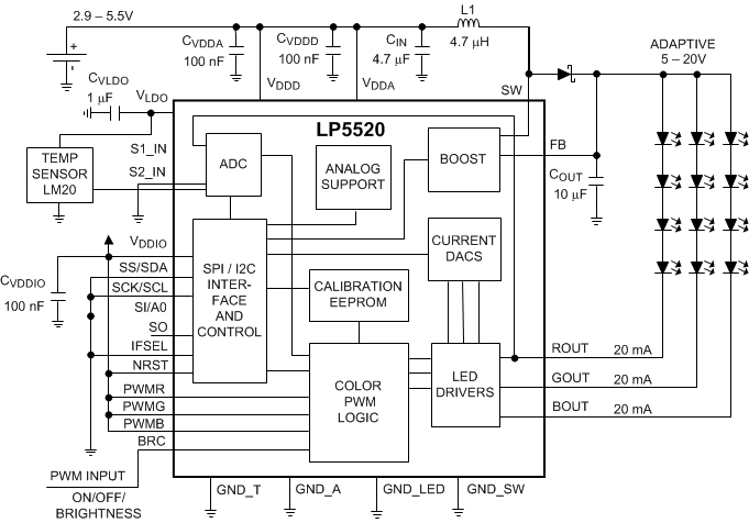
The LP5520 is an RGB backlight LED driver for small format color LCDs. The device has a magnetic boost converter that creates an up to 20-V LED supply voltage from the battery voltage. Three current sinks can drive up to 60 mA of current per string. Figure 32 and Figure 35 show the connections when using LP5520 in automatic mode and in stand-alone mode.
8.2 Typical Applications
8.2.1 Typical Application: I2C-Bus Control
In this typical application LP5520 is controlled with an I2C bus. Operation mode is automatic without external PWM control.
 Figure 32. LP5520 Typical I2C-Bus Application
8.2.1.1 Design Requirements
For typical RGB backlight LED-driver I2C-bus applications, use the parameters listed in Table 14.
Table 14. Design Parameters
| DESIGN PARAMETER | EXAMPLE VALUE |
|---|---|
| Input voltage range | 2.9 V to 5.5 V |
| Maximum output voltage | 20 V |
| LED configuration | 3 strings with 6 LEDs in series |
| LED current | Maximum 60 mA per string |
| Brightness control | I2C |
| Operation mode | Automatic/normal |
| Input capacitor | 10 µF, 6.3 V |
| Output capacitors | 2 × 4.7 µF, 25 V |
| Inductor | 4.7 µH |
| Temperature sensor | LM20 |
8.2.1.2 Detailed Design Procedure
8.2.1.2.1 Recommended External Components
8.2.1.2.1.1 Output Capacitor: COUT
The output capacitor COUT directly affects the magnitude of the output ripple voltage. In general, the higher the value of COUT, the lower the output ripple magnitude. Multilayer ceramic capacitors with low ESR are the best choice. Capacitor voltage rating must be sufficient; TI recommends 25 V or greater. Examples of suitable capacitors are: TDK C3216X5R1E475K, Panasonic ECJ3YB1E475K, and Panasonic ECJ4YB1E475K.
Some ceramic capacitors, especially those in small packages, exhibit a strong capacitance reduction with the increased applied voltage (DC bias effect). The capacitance value can fall below half of the nominal capacitance. Output capacitance that is too low can make the boost converter unstable. Output capacitor value reduction due to DC bias must be less than 70% at 20 V (minimum 3 µF of real capacitance remaining).
8.2.1.2.1.2 Input Capacitor: CIN
The input capacitor CIN directly affects the magnitude of the input ripple voltage and to a lesser degree the VOUT ripple. A higher value CIN gives a lower VIN ripple.
8.2.1.2.1.3 Output Diode: DOUT
A schottky diode must be used for the output diode. To maintain high efficiency the average current rating of the Schottky diode must be greater than the peak inductor current (1 A). Schottky diodes with a low forward drop and fast switching speeds are ideal for increasing efficiency in portable applications. Choose a reverse breakdown voltage of the schottky diode significantly larger (approximately 30 V) than the output voltage. Do not use ordinary rectifier diodes, because slow switching speeds and long recovery times cause the efficiency and the load regulation to suffer. A schottky diode with low parasitic capacitance helps in reducing EMI noise. Examples of suitable diodes are Central Semiconductor CMMSH1-40 and Infineon BAS52-02V.
8.2.1.2.1.4 EMI Filter Components: CSW, RSW, LSW And CHF
EMI filter (RSW, CSW and LSW ) on the SW pin may be needed to slow down the fast switching edges and reduce ringing. These components must be as near as possible to the SW pin to ensure reliable operation. High frequency capacitor (CSW) in the boost output helps in suppressing the high frequency noise from the switcher. 50V or greater voltage rating is recommended for the capacitors. The ferrite bead DC resistance must be less than 0.1 Ω and current rating 1 A or above. The impedance at 100 MHz must be from 30 Ω to 300 Ω. Examples of suitable types are TDK MPZ1608S101A and Taiyo-Yuden FBMH 1608HM600-T.
8.2.1.2.1.5 Inductor: L1
A 4.7-µH shielded inductor is suggested for LP5520 boost converter. The inductor must have a higher saturation current rating than the peak current it receives during circuit operation (0.5 A – 1 A depending on the output current). Equivalent series resistance (ESR) less than 500-mΩ is suggested for high efficiency. Open core inductors cause flux linkage with circuit components and interfere with the normal operation of the circuit. This must be avoided. For high efficiency, choose an inductor with a high-frequency core material such as ferrite to reduce the core losses. To minimize radiated noise, use a toroid, pot core or shielded core inductor. The inductor must be connected to the SW pin as close to the device as possible. Examples of suitable inductors are: TDK VLF3010AT-4R7MR70 and Coilcraft LPS3010-472NL.
8.2.1.2.1.6 List Of Recommended External Components
| SYMBOL | SYMBOL EXPLANATION | VALUE | UNIT | TYPE |
|---|---|---|---|---|
| CVDDA | C between VDDA and GND | 100 | nF | Ceramic, X7R / X5R |
| CVDDD | C between VDDD and GND | 100 | nF | Ceramic, X7R, X5R |
| CVLDO | C between VLDO and GND | 1 | µF | Ceramic, X7R / X5R |
| CVDDIO | C between VDDIO and GND | 100 | nF | Ceramic, X7R / X5R |
| COUT | C between FB and GND | 2 × 4.7 | µF | Ceramic, X7R / X5R, tolerance ±10%, DC bias effect approximately 30% at 20 V |
| CIN | C between battery voltage and GND | 10 | µF | Ceramic, X7R / X5R |
| L1 | L between SW and VBAT | 4.7 | µH | Shielded, low ESR, ISAT 0.5 A |
| D1 | Rectifying diode (Vƒ at maximum load) | 0. 3 – 0.5 | V | Schottky diode, reverse voltage 30 V, repetitive peak current 0.5 A |
| CSW | Optional C in EMI filter | 330 | pF | Ceramic, X7R / X5R, 50V |
| RSW | Optional R in EMI filter | 3.9 | Ω | ±1% |
| CHF | Optional high frequency output C | 33 - 100 | pF | Ceramic, X7R, X5R, 50V |
| LSW | Ferrite bead in SW pin | 30 - 300 | Ω at 100 Mhz |
|
| LEDs | User Defined | |||
8.2.1.3 Application Curves
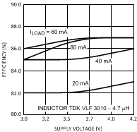
 Figure 33. Boost Converter Efficiency
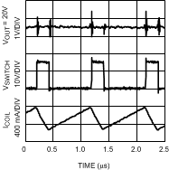
 Figure 34. Boost Typical Waveforms at 60-mA Load
8.2.2 Stand-Alone Typical Application
In stand-alone mode the operation is controlled through a single PWM brightness input, BRC. After power-up or reset the LP5520 is ready for stand-alone operation without any setup through the serial interface. The stand- alone mode is entered with a rising edge in the BRC input. The boost converter operates in adaptive mode. The LED current settings are read from EEPROM. The LED brightness is controlled with a PWM signal in the BRC input. The BRC PWM frequency must be between 2 and 10 kHz.
 Figure 35. Typical Stand-Alone Application
8.2.2.1 Design Requirements
For typical RGB backlight LED-driver stand-alone applications, use the parameters listed in Table 14.
Table 15. Design Parameters
| DESIGN PARAMETER | EXAMPLE VALUE |
|---|---|
| Input voltage range | 2.9 V to 5.5 V |
| Maximum output voltage | 20 V |
| LED configuration | 3 strings with 6 LEDs in series |
| LED current | Maximum 60 mA per string |
| Brightness control | With BRC input, 2-kHz PWM signal; 8 steps |
| Operation mode | Stand-alone operation |
| Input capacitor | 10 µF, 6.3 V |
| Output capacitors | 2 × 4.7 µF, 25 V |
| Inductor | 4.7 µH |
| Temperature sensor | LM20 |
8.2.2.2 Detailed Design Procedure
8.2.2.3 Application Curves
See Application Curves.