SNVS673E April 2010 – September 2014 LP8551
PRODUCTION DATA.
- 1 Features
- 2 Applications
- 3 Description
- 4 Revision History
- 5 Device Default Values
- 6 Pin Configuration and Functions
-
7 Specifications
- 7.1 Absolute Maximum Ratings
- 7.2 Handling Ratings
- 7.3 Recommended Operating Conditions
- 7.4 Thermal Information
- 7.5 Electrical Characteristics
- 7.6 Boost Converter Electrical Characteristics
- 7.7 LED Driver Electrical Characteristics
- 7.8 PWM Interface Characteristics
- 7.9 Undervoltage Protection
- 7.10 Logic Interface Characteristics
- 7.11 I2C Serial Bus Timing Parameters (SDA, SCLK)
- 7.12 Typical Characteristics
-
8 Detailed Description
- 8.1 Overview
- 8.2 Functional Block Diagram
- 8.3
Feature Description
- 8.3.1 Clock Generation
- 8.3.2
Brightness Control Methods
- 8.3.2.1 PWM Input Duty Cycle
- 8.3.2.2 Brightness Register Control
- 8.3.2.3 PWM Direct Control
- 8.3.2.4 PWM Calculation Data Flow
- 8.3.2.5 PWM Detector
- 8.3.2.6 Brightness Control
- 8.3.2.7 Resolution Selector
- 8.3.2.8 Sloper
- 8.3.2.9 PWM Comparator
- 8.3.2.10 Current Setting
- 8.3.2.11 PWM Frequency Setting
- 8.3.2.12 Phase Shift PWM (PSPWM) Scheme
- 8.3.2.13 Slope
- 8.3.2.14 Driver Headroom Control
- 8.3.3 Boost Converter
- 8.3.4 Fault Detection
- 8.4 Device Functional Modes
- 8.5 Programming
- 8.6 Register Map
- 9 Application and Implementation
- 10Power Supply Recommendations
- 11Layout
- 12Device and Documentation Support
- 13Mechanical, Packaging, and Orderable Information
Package Options
Mechanical Data (Package|Pins)
- YZR|25
Thermal pad, mechanical data (Package|Pins)
Orderable Information
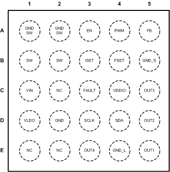
6 Pin Configuration and Functions
DSBGA
25
Top View
DSBGA
25
Bottom View
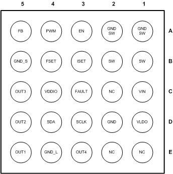
Pin Functions
| PIN | TYPE(1) | DESCRIPTION | |
|---|---|---|---|
| NUMBER | NAME | ||
| A1 | GND_SW | G | Boost switch ground |
| A2 | GND_SW | G | Boost switch ground |
| A3 | EN | I | Enable input pin |
| A4 | PWM | A | PWM dimming input. This pin must be connected to GND if not used. |
| A5 | FB | A | Boost feedback input |
| B1 | SW | A | Boost switch |
| B2 | SW | A | Boost switch |
| B3 | ISET | A | Set resistor for LED current. This pin can be left floating if not used. |
| B4 | FSET | A | PWM frequency set resistor. This pin can be left floating if not used. |
| B5 | GND_S | G | Signal ground |
| C1 | VIN | P | Input power supply up to 22 V. If 2.7 V ≤ VBATT < 5.5 V (Figure 25) then an external 5-V rail must be used for VLDO and VIN. |
| C2 | NC | - | Not connected |
| C3 | FAULT | OD | Fault indication output. If not used, can be left floating. |
| C4 | VDDIO | P | Digital IO reference voltage (1.65 V to 5 V) for I2C interface. If brightness is controlled with PWM input pin then this pin can be connected to GND. |
| C5 | OUT3 | A | Current sink output |
| D1 | VLDO | P | LDO output voltage. External 5-V rail can be connected to this pin in low voltage application. |
| D2 | GND | G | Ground |
| D3 | SCLK | I | Serial clock. This pin must be connected to GND if not used. |
| D4 | SDA | I/O | Serial data. This pin must be connected to GND if not used. |
| D5 | OUT2 | A | Current sink output |
| E1 | NC | - | Not connected |
| E2 | NC | - | Not connected |
| E3 | OUT4 | A | Current sink output |
| E4 | GND_L | G | LED ground |
| E5 | OUT1 | A | Current sink output |
(1) A: Analog Pin, G: Ground Pin, P: Power Pin, I: Input Pin, I/O: Input/Output Pin, O: Output Pin, OD: Open Drain Pin