SLLS047N February 1989 – February 2024 MAX232
PRODUCTION DATA
- 1
- 1 Features
- 2 Applications
- 3 Description
- 4 Pin Configuration and Functions
-
5 Specifications
- 5.1 Absolute Maximum Ratings #GUID-74EA713C-9196-4407-89E7-009CE1353C64/SLLS8089284
- 5.2 ESD Ratings
- 5.3 Recommended Operating Conditions
- 5.4 Thermal Information
- 5.5 Electrical Characteristics, Device
- 5.6 Electrical Characteristics, Driver
- 5.7 Electrical Characteristics, Receiver
- 5.8 Switching Characteristics
- 5.9 Typical Characteristics
- 6 Parameter Measurement Information
- 7 Detailed Description
- 8 Application and Implementation
- 9 Device and Documentation Support
- 10Revision History
- 11Mechanical, Packaging, and Orderable Information
Package Options
Refer to the PDF data sheet for device specific package drawings
Mechanical Data (Package|Pins)
- NS|16
- DW|16
- N|16
- D|16
Thermal pad, mechanical data (Package|Pins)
Orderable Information
3 Description
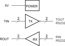
The MAX232 device is a dual driver/receiver that includes a capacitive voltage generator to supply TIA/EIA-232-F voltage levels from a single 5V supply. Each receiver converts TIA/EIA-232-F inputs to 5V TTL/CMOS levels. These receivers have a typical threshold of 1.3 V, a typical hysteresis of 0.5V, and can accept ±30V inputs. Each driver converts TTL/CMOS input levels into TIA/EIA-232-F levels.
Package
Information
| PART NUMBER | PACKAGE(1) | PACKAGE SIZE(2) |
|---|---|---|
| MAX232 | SOIC (16) | 9.9mm × 6mm |
| SOIC (16) | 10.4mm × 10.3mm | |
| PDIP (16) | 19.3mm × 9mm | |
| SOP (16) | 10.2mm × 7.8 mm |
(1) For more Information, see Section 11 .
(2) The package size (length × width)
is a nominal value and includes pins, where applicable.
 Simplified Schematic