SLLS408H January 2000 – October 2016 MAX3222
PRODUCTION DATA.
- 1 Features
- 2 Applications
- 3 Description
- 4 Revision History
- 5 Pin Configuration and Functions
-
6 Specifications
- 6.1 Absolute Maximum Ratings
- 6.2 ESD Ratings
- 6.3 Recommended Operating Conditions
- 6.4 Thermal Information
- 6.5 Electrical Characteristics: Device
- 6.6 Electrical Characteristics: Driver
- 6.7 Electrical Characteristics: Receiver
- 6.8 Switching Characteristics: Driver
- 6.9 Switching Characteristics: Receiver
- 6.10 Typical Characteristics
- 7 Parameter Measurement Information
- 8 Detailed Description
- 9 Application and Implementation
- 10Power Supply Recommendations
- 11Layout
- 12Device and Documentation Support
- 13Mechanical, Packaging, and Orderable Information
Package Options
Refer to the PDF data sheet for device specific package drawings
Mechanical Data (Package|Pins)
- PW|20
Thermal pad, mechanical data (Package|Pins)
Orderable Information
9 Application and Implementation
NOTE
Information in the following applications sections is not part of the TI component specification, and TI does not warrant its accuracy or completeness. TI’s customers are responsible for determining suitability of components for their purposes. Customers should validate and test their design implementation to confirm system functionality.
9.1 Application Information
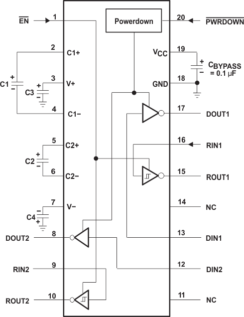
The MAX3222 interfaces a universal asynchronous receiver / transmitter (UART) to RS-232 port voltage levels. External capacitors are used to generate RS-232 compliant voltages. For proper operation, add capacitors as shown in Figure 8.
9.2 Typical Application
ROUT and DIN connect to UART or general purpose logic lines. RIN and DOUT lines connect to a RS232 connector or cable.

9.2.1 Design Requirements
- Recommended VCC is 3.3 V or 5 V. 3 V to 5.5 V is also possible
- Maximum recommended bit rate is 250 kbit/s.
Table 3. VCC vs Capacitor Values
| VCC | C1 | C2, C3, and C4 |
|---|---|---|
| 3.3 V ± 0.3 V | 0.1 µF | 0.1 µF |
| 5 V ± 0.5 V | 0.047 µF | 0.33 µF |
| 3 V ± 5.5 V | 0.1 µF | 0.47 µF |
9.2.2 Detailed Design Procedure
- All DIN, PWRDOWN and EN inputs must be connected to valid low or high logic levels.
- Select capacitor values based on VCC level for best performance.
9.2.3 Application Curves
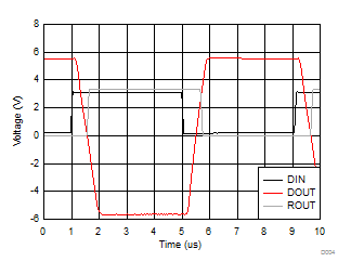
 Figure 9. Loopback Waveforms
VCC = 3.3 V, Data Rate 250 kbit/s
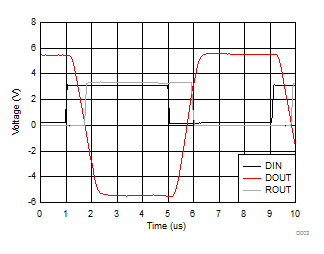
 Figure 10. Loopback Waveforms with 1-nF load
VCC = 3.3 V, Data Rate 250 kbit/s