SLLS408H January 2000 – October 2016 MAX3222
PRODUCTION DATA.
- 1 Features
- 2 Applications
- 3 Description
- 4 Revision History
- 5 Pin Configuration and Functions
-
6 Specifications
- 6.1 Absolute Maximum Ratings
- 6.2 ESD Ratings
- 6.3 Recommended Operating Conditions
- 6.4 Thermal Information
- 6.5 Electrical Characteristics: Device
- 6.6 Electrical Characteristics: Driver
- 6.7 Electrical Characteristics: Receiver
- 6.8 Switching Characteristics: Driver
- 6.9 Switching Characteristics: Receiver
- 6.10 Typical Characteristics
- 7 Parameter Measurement Information
- 8 Detailed Description
- 9 Application and Implementation
- 10Power Supply Recommendations
- 11Layout
- 12Device and Documentation Support
- 13Mechanical, Packaging, and Orderable Information
Package Options
Refer to the PDF data sheet for device specific package drawings
Mechanical Data (Package|Pins)
- PW|20
Thermal pad, mechanical data (Package|Pins)
Orderable Information
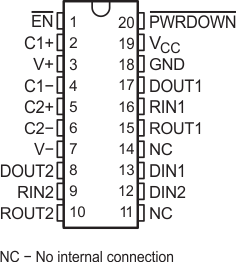
5 Pin Configuration and Functions
Pin Functions
| PIN | I/O | DESCRIPTION | |
|---|---|---|---|
| NAME | NO. | ||
| C1+ | 2 | — | Charge pump capacitor pin |
| C1- | 4 | — | Charge pump capacitor pin |
| C2+ | 5 | — | Charge pump capacitor pin |
| C2- | 6 | — | Charge pump capacitor pin |
| DIN1 | 13 | I | Driver logic input |
| DIN2 | 12 | I | Driver logic input |
| DOUT1 | 17 | O | RS-232 driver output |
| DOUT2 | 8 | O | RS-232 driver output |
| EN | 1 | I | Receiver enable, active low |
| GND | 18 | — | Ground |
| NC | 11,14 | — | No internal connection |
| PWRDOWN | 20 | I | Driver disable, active low |
| RIN1 | 16 | I | RS-232 receiver input |
| RIN2 | 9 | I | RS-232 receiver input |
| ROUT1 | 15 | O | Receiver logic output |
| ROUT2 | 10 | O | Receiver logic output |
| VCC | 19 | — | Power Supply |
| V+ | 3 | — | Charge pump capacitor pin |
| V- | 7 | — | Charge pump capacitor pin |
