SBOS777D November   2016  – July 2020 OPA2388 , OPA388 , OPA4388

PRODUCTION DATA  

  1. Features
  2. Applications
  3. Description
  4. Revision History
  5. Pin Configuration and Functions
  6. Specifications
    1. 6.1 Absolute Maximum Ratings
    2. 6.2 ESD Ratings
    3. 6.3 Recommended Operating Conditions
    4. 6.4 Thermal Information: OPA388
    5. 6.5 Thermal Information: OPA2388
    6. 6.6 Thermal Information: OPA4388
    7. 6.7 Electrical Characteristics: VS = ±1.25 V to ±2.75 V (VS = 2.5 to 5.5 V)
    8. 6.8 Typical Characteristics
  7. Detailed Description
    1. 7.1 Overview
    2. 7.2 Functional Block Diagram
    3. 7.3 Feature Description
      1. 7.3.1 Operating Voltage
      2. 7.3.2 Input Voltage and Zero-Crossover Functionality
      3. 7.3.3 Input Differential Voltage
      4. 7.3.4 Internal Offset Correction
      5. 7.3.5 EMI Susceptibility and Input Filtering
    4. 7.4 Device Functional Modes
  8. Application and Implementation
    1. 8.1 Application Information
    2. 8.2 Typical Applications
      1. 8.2.1 Bidirectional Current-Sensing
        1. 8.2.1.1 Design Requirements
        2. 8.2.1.2 Detailed Design Procedure
        3. 8.2.1.3 Application Curve
      2. 8.2.2 Single Operational Amplifier Bridge Amplifier
      3. 8.2.3 Precision, Low-Noise, DAC Buffer
      4. 8.2.4 Load Cell Measurement
  9. Power Supply Recommendations
  10. 10Layout
    1. 10.1 Layout Guidelines
    2. 10.2 Layout Example
  11. 11Device and Documentation Support
    1. 11.1 Device Support
      1. 11.1.1 Development Support
        1. 11.1.1.1 TINA-TI™ Simulation Software (Free Download)
        2. 11.1.1.2 TI Precision Designs
    2. 11.2 Documentation Support
      1. 11.2.1 Related Documentation
    3. 11.3 Related Links
    4. 11.4 Receiving Notification of Documentation Updates
    5. 11.5 Support Resources
    6. 11.6 Trademarks
    7. 11.7 Electrostatic Discharge Caution
    8. 11.8 Glossary
  12. 12Mechanical, Packaging, and Orderable Information

Package Options

Mechanical Data (Package|Pins)
Thermal pad, mechanical data (Package|Pins)
Orderable Information

Input Differential Voltage

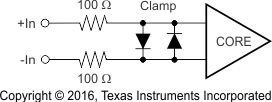
The typical input bias current of the OPAx388 during normal operation is approximately 30 pA. In overdriven conditions, the bias current can increase significantly. The most common cause of an overdriven condition occurs when the operational amplifier is outside of the linear range of operation. When the output of the operational amplifier is driven to one of the supply rails, the feedback loop requirements cannot be satisfied and a differential input voltage develops across the input pins. This differential input voltage results in activation of parasitic diodes inside the front-end input chopping switches that combine with 10-kΩ electromagnetic interference (EMI) filter resistors to create the equivalent circuit shown in Figure 7-4. Notice that the input bias current remains within specification in the linear region.
GUID-5C55CD11-93AD-4426-823D-4054B2E04091-low.gifFigure 7-4 Equivalent Input Circuit