SBOS794 December 2016 OPA2836-Q1
PRODUCTION DATA.
- 1 Features
- 2 Applications
- 3 Description
- 4 Revision History
- 5 OPA2836-Q1 Related Devices
- 6 Pin Configuration and Functions
- 7 Specifications
- 8 Detailed Description
-
9 Application and Implementation
- 9.1
Application Information
- 9.1.1 Noninverting Amplifier
- 9.1.2 Inverting Amplifier
- 9.1.3 Instrumentation Amplifier
- 9.1.4 Attenuators
- 9.1.5 Single-Ended-to-Differential Amplifier
- 9.1.6 Differential-to-Signal-Ended Amplifier
- 9.1.7 Differential-to-Differential Amplifier
- 9.1.8 Pulse Application With Single-Supply
- 9.1.9 ADC Driver Performance
- 9.2 Typical Applications
- 9.1
Application Information
- 10Power Supply Recommendations
- 11Layout
- 12Device and Documentation Support
- 13Mechanical, Packaging, and Orderable Information
Package Options
Mechanical Data (Package|Pins)
- DGK|8
Thermal pad, mechanical data (Package|Pins)
- DGK|8
Orderable Information
8 Detailed Description
8.1 Overview
The OPA2836-Q1 bipolar input operational amplifier offers an excellent bandwidth of 205 MHz with ultra-low THD of 0.00003% at 1 kHz. The OPA2836-Q1 can swing to within 200 mV of the supply rails when driving a
1-kΩ load. The input common-mode of the amplifier can swing to 200 mV below the negative supply rail. This level of performance is achieved at 1 mA of quiescent current per amplifier channel.
8.2 Functional Block Diagrams
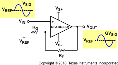 Figure 51. Noninverting Amplifier
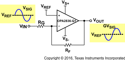 Figure 52. Inverting Amplifier
8.3 Feature Description
8.3.1 Input Common-Mode Voltage Range
When the primary design goal is a linear amplifier with high CMRR, the input common-mode voltage range (VICR) of the amplifier must not be violated.
The common-mode input range low and high specifications are based on CMRR. The specification limits are chosen to ensure CMRR does not degrade more than 3 dB below the mid-supply limit if the input voltage is kept within the specified range. The limits cover all process variations and most parts are better than specified. The typical specifications are from 0.2 V below the negative rail to 1.1 V below the positive rail.
Given that the operational amplifier is in linear operation, the voltage difference between the input pins is very small (ideally 0 V), and input common-mode voltage can be analyzed at either input pin with the other input pin assumed to be at the same potential. The voltage at VIN+ is easy to evaluate. In the noninverting configuration, Figure 51, the input signal VIN must not violate VICR. In the inverting configuration, Figure 52, the reference voltage VREF must be within VICR.
The input voltage limits have a fixed headroom to the power rails and track the power-supply voltages. For one 5-V supply, the linear input voltage range is –0.2 V to 3.9 V, and with a 2.7-V supply this range is –0.2 V to 1.6 V. The delta from each power-supply rail is the same in either case: –0.2 V and 1.1 V.
8.3.2 Output Voltage Range
The OPA2836-Q1 is a rail-to-rail output (RRO) operational amplifier. Rail-to-rail output typically means the output voltage can swing to within a couple hundred millivolts of the supply rails. There are two different ways to specify this: with the output still in linear operation and with the output saturated. Saturated output voltages are closer to the power-supply rails than linear outputs, but the signal is not a linear representation of the input. Linear output is a better representation of how well a device performs when used as a linear amplifier. Both saturation and linear operation limits are affected by the current in the output, where higher currents lead to more loss in the output transistors.
Data in the Electrical Characteristics tables list both linear and saturated output voltage specifications with a 1-kΩ load. Figure 11 and Figure 36 illustrate saturated voltage-swing limits versus output load resistance, and Figure 12 and Figure 37 illustrate the output saturation voltage versus load current. Given a light load, the output voltage limits have a nearly constant headroom to the power rails and track the power-supply voltages. For example, with a 2-kΩ load and a single 5-V supply, the linear output voltage range is 0.15 V to 4.8 V, and with a 2.7-V supply this range is 0.15 V to 2.5 V. The delta from each power-supply rail is the same in either case: 0.15 V and 0.2 V.
With devices such as the OPA2836-Q1 where the input range is lower than the output range, the input typically limits the available signal swing only in the noninverting gain of 1. Signal swings in noninverting configurations in gains greater than +1 and in inverting configurations in any gain are generally limited by the output voltage limits of the operational amplifier.
8.3.3 Low-Power Applications and the Effects of Resistor Values on Bandwidth
The OPA2836-Q1 is designed for the nominal value of RF to be 1 kΩ in gains other than +1 V/V. This value of RF = 1 kΩ gives excellent distortion performance, maximum bandwidth, best flatness, and best pulse response. This value also loads the amplifier. For example, in a gain of 2 with RF = RG = 1 kΩ, RG to ground, and VOUT = 4 V, 2 mA of current flows through the feedback path to ground. In s gain of +1, RG is open and no current flows to ground. In low-power applications, reducing this current by increasing the gain-setting resistors values is desirable. Using larger value gain resistors has two primary side effects (other than lower power) because of the interaction with parasitic circuit capacitance:
- Lowers the bandwidth
- Lowers the phase margin
- Causes peaking in the frequency response
- Also causes overshoot and ringing in the pulse response
Figure 53 shows the small-signal frequency response for a noninverting gain of 2 with RF and RG equal to 1 kΩ, 10 kΩ, and 100 kΩ. The test was done with RL = 1 kΩ. Lower values can reduce the peaking because of loading effects of RL, but higher values do not have a significant effect.
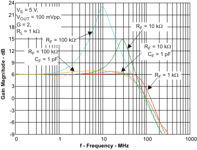 Figure 53. Frequency Response With Various Gain-Setting Resistor Values
As expected, larger value gain resistors cause lower bandwidth and peaking in the response (peaking in the frequency response is synonymous with overshoot and ringing in pulse response). Adding 1-pF capacitors in parallel with RF helps compensate the phase margin and restores flat frequency response. Figure 54 shows the test circuit used.
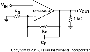 Figure 54. G = 2 Test Circuit for Various Gain-Setting Resistor Values
8.3.4 Driving Capacitive Loads
The OPA2836-Q1 can drive up to a nominal capacitive load of 2.2 pF on the output with no special consideration. When driving capacitive loads greater than this load, using a small resister (RO) in series with the output as close to the device as possible is recommended. Without RO, the capacitance on the output interacts with the output impedance of the amplifier causing phase shift in the loop gain of the amplifier that reduces the phase margin. This scenario causes peaking in the frequency response and overshoot and ringing in the pulse responses. Interaction with other parasitic elements can lead to instability or oscillation. Inserting RO isolates the phase shift from the loop-gain path and restores the phase margin; however, the bandwidth is also limited.
Figure 55 shows the test circuit and Figure 42 illustrates the recommended values of RO versus capacitive loads, CL. See Figure 39 for frequency responses with various values.
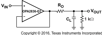 Figure 55. RO versus CL Test Circuit
8.4 Device Functional Modes
8.4.1 Split-Supply Operation (±1.25 V to ±2.75 V)
To facilitate testing with common lab equipment, the OPA2836-Q1 EVM (see the OPA835DBV, OPA836DBV EVM, SLOU314) is built to allow for split-supply operation. This configuration eases lab testing because the mid-point between the power rails is ground, and most signal generators, network analyzers, oscilloscopes, spectrum analyzers, and other lab equipment reference inputs and outputs to ground.
Figure 56 shows a simple noninverting configuration analogous to Figure 51 with a ±2.5-V supply and VREF equal to ground. The input and output swing symmetrically around ground. Split-supply operation is preferred because of the ease of use in systems where signals swing around ground, but two supply rails still must be generated.
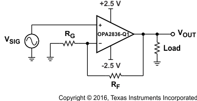 Figure 56. Split-Supply Operation
8.4.2 Single-Supply Operation (2.5 V to 5.5 V)
Many newer systems use a single power supply to improve efficiency and reduce the cost of the power supply. The OPA2836-Q1 is designed for use with single-supply power operation and can be used with single-supply power with no change in performance from split supply as long as the input and output are biased within the linear operation of the device.
To change the circuit from split supply to single supply, level shift all voltages by half the difference between the power-supply rails. For example, changing from a ±2.5-V split supply to a 5-V single supply is shown conceptually in Figure 57.
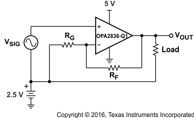 Figure 57. Single Supply Concept
A more practical circuit has a prior amplifier or another circuit to provide the bias voltage for the input with the output providing the bias for the next stage.
Figure 58 shows a typical noninverting amplifier situation. With a 5-V single supply, a mid-supply reference generator is needed to bias the negative side through RG. To cancel the voltage offset that is otherwise caused by the input bias currents, R1 is chosen to be equal to RF in parallel with RG. For example, if a gain of 2 is required and RF = 1 kΩ, select RG = 1 kΩ to set the gain and R1 = 499 Ω for bias current cancellation. The value for C is dependent on the reference, but at least 0.1 µF is recommended to limit noise.
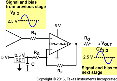 Figure 58. Noninverting Single Supply With Reference
Figure 59 shows a similar noninverting single-supply scenario with the reference generator replaced by the Thevenin equivalent using resistors and the positive supply. RG’ and RG” form a resistor divider from the 5-V supply and are used to bias the negative side with the parallel sum equal to the equivalent RG to set the gain. To cancel the voltage offset that is otherwise caused by the input bias currents, R1 is chosen to be equal to RF in parallel with RG’ in parallel with RG” (R1= RF || RG’ || RG”). For example, if a gain of 2 is required and RF = 1 kΩ, selecting RG’ = RG” = 2 kΩ gives an equivalent parallel sum of 1 kΩ, sets the gain to 2, and references the input to mid supply (2.5 V). R1 is then set to 499 Ω for bias current cancellation, which can be lower cost compared to Figure 59 but requires extra current in the resistor divider.
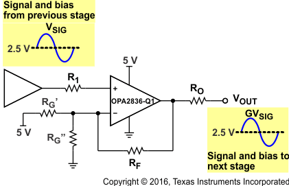 Figure 59. Noninverting Single Supply With Resistors
Figure 60 shows a typical inverting amplifier situation. With a 5-V single supply, a mid-supply reference generator is needed to bias the positive side via R1. To cancel the voltage offset that is otherwise caused by the input bias currents, R1 is chosen to be equal to RF in parallel with RG. For example, if a gain of –2 is required and RF = 1 kΩ, select RG = 499 Ω to set the gain and R1 = 332 Ω for bias-current cancellation. The value for C is dependent on the reference, but at least 0.1 µF is recommended to limit noise into the operational amplifier.
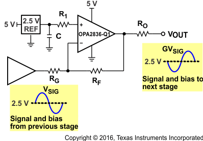 Figure 60. Inverting Single Supply With Reference
Figure 61 shows a similar inverting single-supply scenario with the reference generator replaced by the Thevenin equivalent using resistors and the positive supply. R1 and R2 form a resistor divider from the 5-V supply and are used to bias the positive side. To cancel the voltage offset that is otherwise caused by the input bias currents, set the parallel sum of R1 and R2 equal to the parallel sum of RF and RG. C must be added to limit coupling of noise into the positive input. For example, if a gain of –2 is required and RF = 1 kΩ, select RG = 499 Ω to set the gain. R1 = R2 = 665 Ω for mid-supply voltage bias and for operational amplifier input bias current cancellation. A good value for C is 0.1 µF and can be a lower cost compared to Figure 61, but requires extra current in the resistor divider.
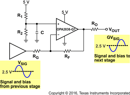 Figure 61. Inverting Single Supply With Resistors