SBOS794 December 2016 OPA2836-Q1
PRODUCTION DATA.
- 1 Features
- 2 Applications
- 3 Description
- 4 Revision History
- 5 OPA2836-Q1 Related Devices
- 6 Pin Configuration and Functions
- 7 Specifications
- 8 Detailed Description
-
9 Application and Implementation
- 9.1
Application Information
- 9.1.1 Noninverting Amplifier
- 9.1.2 Inverting Amplifier
- 9.1.3 Instrumentation Amplifier
- 9.1.4 Attenuators
- 9.1.5 Single-Ended-to-Differential Amplifier
- 9.1.6 Differential-to-Signal-Ended Amplifier
- 9.1.7 Differential-to-Differential Amplifier
- 9.1.8 Pulse Application With Single-Supply
- 9.1.9 ADC Driver Performance
- 9.2 Typical Applications
- 9.1
Application Information
- 10Power Supply Recommendations
- 11Layout
- 12Device and Documentation Support
- 13Mechanical, Packaging, and Orderable Information
Package Options
Mechanical Data (Package|Pins)
- DGK|8
Thermal pad, mechanical data (Package|Pins)
- DGK|8
Orderable Information
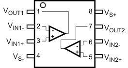
6 Pin Configuration and Functions
DGK Package
8-Pin VSSOP
Top View

Pin Functions
| NAME | PIN | I/O | DESCRIPTION |
|---|---|---|---|
| VIN1+ | 3 | Input | Amplifier 1 noninverting input |
| VIN1– | 2 | Input | Amplifier 1 inverting input |
| VIN2+ | 5 | Input | Amplifier 2 noninverting input |
| VIN2– | 6 | Input | Amplifier 2 inverting input |
| VOUT1 | 1 | Output | Amplifier 1 output |
| VOUT2 | 7 | Output | Amplifier 2 output |
| VS+ | 8 | Power | Positive power supply input |
| VS– | 4 | Power | Negative power supply input |