SBOS365G may   2006  – may 2023 OPA2365 , OPA365

PRODUCTION DATA  

  1.   1
  2. Features
  3. Applications
  4. Description
  5. Revision History
  6. Device Comparison Table
  7. Pin Configuration and Functions
  8. Specifications
    1. 7.1 Absolute Maximum Ratings
    2. 7.2 ESD Ratings
    3. 7.3 Recommended Operating Conditions
    4. 7.4 Thermal Information: OPA365
    5. 7.5 Thermal Information: OPA2365
    6. 7.6 Electrical Characteristics
    7. 7.7 Typical Characteristics
  9. Detailed Description
    1. 8.1 Overview
    2. 8.2 Functional Block Diagram
    3. 8.3 Feature Description
      1. 8.3.1 Rail-to-Rail Input
      2. 8.3.2 Input and ESD Protection
      3. 8.3.3 Capacitive Loads
      4. 8.3.4 Achieving an Output Level of Zero Volts (0 V)
      5. 8.3.5 Active Filtering
    4. 8.4 Device Functional Modes
  10. Application and Implementation
    1. 9.1 Application Information
      1. 9.1.1 Basic Amplifier Configurations
    2. 9.2 Typical Application
      1. 9.2.1 Design Requirements
      2. 9.2.2 Detailed Design Procedure
      3. 9.2.3 Application Curve
    3. 9.3 System Examples
      1. 9.3.1 Driving an Analog-to-Digital Converter
    4. 9.4 Power Supply Recommendations
    5. 9.5 Layout
      1. 9.5.1 Layout Guidelines
      2. 9.5.2 Layout Example
  11. 10Device and Documentation Support
    1. 10.1 Device Support
      1. 10.1.1 Development Support
        1. 10.1.1.1 PSpice® for TI
        2. 10.1.1.2 TINA-TI™ Simulation Software (Free Download)
        3. 10.1.1.3 DIP-Adapter-EVM
        4. 10.1.1.4 DIYAMP-EVM
        5. 10.1.1.5 TI Reference Designs
        6. 10.1.1.6 Filter Design Tool
    2. 10.2 Documentation Support
      1. 10.2.1 Related Documentation
    3. 10.3 Receiving Notification of Documentation Updates
    4. 10.4 Support Resources
    5. 10.5 Trademarks
    6. 10.6 Electrostatic Discharge Caution
    7. 10.7 Glossary
  12. 11Mechanical, Packaging, and Orderable Information

Package Options

Mechanical Data (Package|Pins)
Thermal pad, mechanical data (Package|Pins)
Orderable Information

Input and ESD Protection

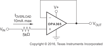
The OPAx365 devices incorporate internal electrostatic discharge (ESD) protection circuits on all pins. In the case of input and output pins, this protection primarily consists of current steering diodes connected between the input and power-supply pins. These ESD protection diodes also provide in-circuit, input overdrive protection, provided that the current is limited to 10 mA, as stated in Section 7.1. Figure 8-2 shows how a series input resistor can be added to the driven input to limit the input current. The added resistor contributes thermal noise at the amplifier input and the value must be kept to the minimum in noise-sensitive applications.
GUID-00674D3A-DA42-4A0B-B0C3-FF3482E3ACB0-low.gifFigure 8-2 Input Current Protection