SBOS365G may 2006 – may 2023 OPA2365 , OPA365
PRODUCTION DATA
- 1
- 1 Features
- 2 Applications
- 3 Description
- 4 Revision History
- 5 Device Comparison Table
- 6 Pin Configuration and Functions
- 7 Specifications
- 8 Detailed Description
- 9 Application and Implementation
- 10Device and Documentation Support
- 11Mechanical, Packaging, and Orderable Information
Package Options
Mechanical Data (Package|Pins)
Thermal pad, mechanical data (Package|Pins)
Orderable Information
8.3.4 Achieving an Output Level of Zero Volts (0 V)
Certain single-supply applications require the op amp output to swing from 0 V to a positive full-scale voltage and have high accuracy. An example is an op amp employed to drive a single-supply ADC having an input range from 0 V to 5 V. Rail-to-rail output amplifiers with very light output loading can achieve an output level within millivolts of 0 V (or +VS at the high end), but not 0 V. Furthermore, the deviation from 0 V only becomes greater as the load current required increases. This increased deviation is a result of limitations of the CMOS output stage.
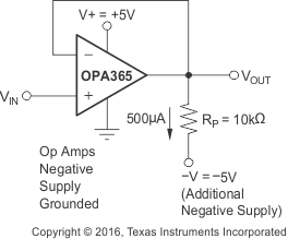
When a pulldown resistor is connected from the amplifier output to a negative voltage source, the OPAx365 can achieve an output level of 0 V, and even a few millivolts below 0 V. Below this limit, nonlinearity and limiting conditions become evident. Figure 8-4 illustrates a circuit using this technique.
A pulldown current of approximately 500 μA is required when the OPAx365 is connected as a unity-gain buffer. A practical termination voltage (VNEG) is −5 V, but other convenient negative voltages also can be used. Pulldown resistor RL is calculated from RL = [(VO − VNEG) / (500 μA)].
Using a minimum output voltage (VO) of 0 V, RL = [0 V − (−5 V)] / (500 μA)] = 10 kΩ. Keep in mind that lower termination voltages result in smaller pulldown resistors that load the output during positive output voltage excursions.
This technique does not work with all op amps; apply only to op amps such as the OPAx365 that have been specifically designed to operate in this manner. Also, operating the OPAx365 output at 0 V changes the output-stage operating conditions, resulting in somewhat lower open-loop gain and bandwidth.
Keep these precautions in mind when driving a capacitive load because these conditions can affect circuit transient response and stability.
 Figure 8-4 Swing-to-Ground